8-LED bar and chaser effects
Drive a row of eight LEDs (Knight Rider scanner, VU-style bar, binary counter) from just three Arduino pins using shiftOut().
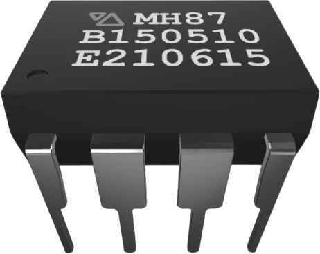
The 74HC595 is an 8-bit serial-in, parallel-out shift register that turns three microcontroller pins into eight latched outputs.
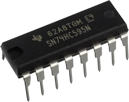
The SN74HC595 is an 8-bit serial-in, parallel-out shift register with a separate storage (latch) register and 3-state outputs. It lets a microcontroller drive eight outputs (QA through QH) using just three signal pins: serial data (SER), a shift clock (SRCLK), and a latch clock (RCLK). That makes it one of the most common ways to expand the number of digital outputs on an Arduino or similar board.
Internally the chip holds two registers. Data on SER is clocked into the 8-bit shift register on each rising edge of SRCLK, moving through one stage at a time. The shift register contents are copied to the storage register, and appear on the parallel outputs, only on a rising edge of RCLK. Because the outputs update from the latch, all eight pins change at once with no visible ripple as the bits shift in. The active-low /OE pin either enables the outputs or puts them into high impedance, and the active-low /SRCLR pin clears the shift register.
The QH' (Q7S) pin mirrors the last stage of the shift register, so multiple 74HC595s can be daisy-chained to control 16, 24, or more outputs from the same three control lines. The device operates across a wide 2V to 6V supply, so it works directly with both 5V and 3.3V logic.
| Pin | Function | Type |
|---|---|---|
QB 1 QB | Digital parallel output B | Digital output |
QC 2 QC | Digital parallel output C | Digital output |
QD 3 QD | Digital parallel output D | Digital output |
QE 4 QE | Digital parallel output E | Digital output |
QF 5 QF | Digital parallel output F | Digital output |
QG 6 QG | Digital parallel output G | Digital output |
QH 7 QH | Digital parallel output H | Digital output |
GND 8 GND | Power | Power in |
VCC 16 VCC | Power | Power in |
QA 15 QA | Digital parallel output A | Digital output |
SER 14 SER / DS | Digital serial data input | Digital input |
OE 13 /OE | Digital output enable, active low | Digital input |
RCLK 12 RCLK / ST_CP | Digital storage register clock / latch | Digital input |
SRCLK 11 SRCLK / SH_CP | Digital shift register clock | Digital input |
SRCLR 10 /SRCLR / MR | Digital shift register clear, active low | Digital input |
QH_PRIME 9 QH' / Q7S | Digital serial output for cascading | Digital output |
Verified from the Tinkered component library · Texas Instruments.
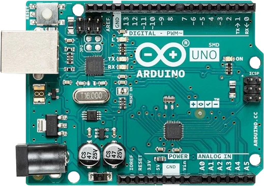
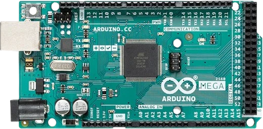
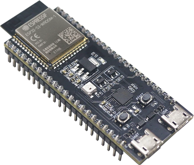
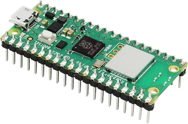
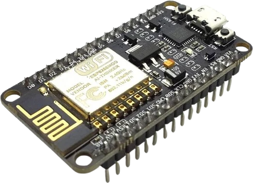
The 74HC595 Shift Register connects to any of the microcontrollers supported in Tinkered. Mind the 5 V logic level on 3.3 V boards.
Shifting bits in with SRCLK does not change the outputs. The storage register only updates on a rising edge of RCLK. If you shift eight bits but never pulse RCLK, the parallel outputs stay frozen at their previous values.
The output enable is active low. If /OE (pin 13) is left unconnected or pulled high, all outputs go high impedance and nothing appears to work even though the registers are shifting correctly. Tie it to GND.
The master reset is active low. If /SRCLR (pin 10) is left floating or accidentally held low, the shift register is continuously cleared and no data can be stored. Tie it to VCC.
With shiftOut(), MSBFIRST versus LSBFIRST determines whether the first bit lands on QH or QA, and QA (pin 15) sits apart from QB through QH (pins 1 to 7). Getting the order wrong lights the wrong outputs; verify the mapping against the pinout.
Driving LEDs without series resistors, or too many outputs at once, can exceed the +/-35mA per-pin and 70mA total device limits. Add current-limiting resistors and budget the combined current across all active outputs.
Drive a row of eight LEDs (Knight Rider scanner, VU-style bar, binary counter) from just three Arduino pins using shiftOut().
Use one 74HC595 per digit to control the segments of multiplexed 7-segment displays without tying up a pin per segment.
Daisy-chain several 595s through QH' to create 16, 24, or more outputs while still using only three control lines from the microcontroller.
Pair shift registers to source columns and sink rows, driving an 8x8 LED matrix for scrolling text and simple animations.
Drop the 74HC595 Shift Register into a circuit, write firmware, and simulate it in your browser, then deploy to real hardware. All in one editable Tinkered project.