74HC165 Shift Register
The 74HC165 is an 8-bit parallel-in, serial-out shift register that reads eight buttons or switches on three microcontroller pins.
- Function8-bit parallel-in, serial-out shift register with clock inhibit and complementary output
- Supply voltage2 V to 6 V (5 V nominal)
- Input high threshold1.5 V at VCC 2 V, 3.15 V at VCC 4.5 V, 4.2 V at VCC 6 V
- Unused inputsMust be held at VCC or GND
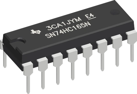
The 74HC165 is an 8-bit parallel-load shift register that reads eight digital inputs (A to H) on three microcontroller pins: SH/LD (pin 1), CLK (pin 2) and the serial output QH (pin 9) (TI SN74HC165 datasheet SCLS116H, p. 3). Power it from the board's own logic supply (it runs from 2 V to 6 V, p. 1), tie CLK INH (pin 15) and SER (pin 10) to GND, and give every input a pull resistor or a rail, because TI requires unused inputs held at VCC or GND (p. 4). Pulse SH/LD low to load, then read QH before each rising CLK edge: H comes out first.
The SN74HC165 is an 8-bit parallel-load shift register: the input twin of the 74HC595. Eight data inputs, A to H, are copied into the register at once while the shift/load pin SH/LD is low, and each rising edge of CLK then moves the register one stage toward the serial output QH (TI SN74HC165 datasheet SCLS116H, pp. 1, 12). A microcontroller reads eight buttons, switches or DIP-switch positions this way with only three pins: one for SH/LD, one for CLK, and one input for QH.
Loading is asynchronous: while SH/LD is low the register follows the parallel inputs and ignores both clock pins, so QH already shows input H the moment the load ends (datasheet, pp. 12, 13). With SH/LD high, a rising edge on CLK shifts while CLK INH is low; CLK and CLK INH are interchangeable, so holding CLK INH high freezes the register (p. 12). Data on the serial input SER enters the first stage on every shift, which is how several chips cascade: the far chip's QH feeds the near chip's SER and all chips share SH/LD and CLK, so 16, 24 or more inputs still need three pins (p. 14). Pin 7 is the complementary output, QH inverted, and can be left open.
The chip runs from 2 V to 6 V, draws 80 µA at most at rest, and clocks to 25 MHz at 4.5 V (datasheet, pp. 1, 7), far faster than any Arduino loop. Its inputs are CMOS with a 3.15 V high threshold at a 4.5 V supply (p. 4), so power it from the same rail as the microcontroller reading it: 5 V beside an Uno, 3.3 V beside an ESP32 or Raspberry Pi Pico. That also keeps QH, which swings to VCC, safe for the reading pin.
74HC165 Shift Register pinout
| Pin | Function | Type |
|---|---|---|
| SH_LD | Digital | input |
| CLK | Digital | input |
| E | Digital | input |
| F | Digital | input |
| G | Digital | input |
| H | Digital | input |
| QH_N | Digital | output |
| GND | 8 GND | power in |
| VCC | 16 VCC (2-6 V)2–5 V | power in |
| CLK_INH | Digital | input |
| D | Digital | input |
| C | Digital | input |
| B | Digital | input |
| A | Digital | input |
| SER | Digital | input |
| QH | Digital | output |
How to wire the 74HC165 Shift Register
Pin by pin, for the board you have.
| 74HC165 Shift Register | Arduino Uno | Note |
|---|---|---|
| VCC | 5V | |
| GND | GND | |
| SH_LD | D8 | |
| CLK | D13 | |
| QH | D12 | |
| CLK_INH | GND | |
| SER | GND | |
| A | GND | through a 10 kΩ resistor |
| B | GND | through a 10 kΩ resistor |
| C | GND | |
| D | GND | |
| E | GND | |
| F | GND | |
| G | GND | |
| H | GND |
| 74HC165 Shift Register | ESP32 DevKit V1 | Note |
|---|---|---|
| VCC | 3V3 | |
| GND | GND | |
| SH_LD | GPIO13 (D13) | |
| CLK | GPIO14 (D14) | |
| QH | GPIO27 (D27) | |
| CLK_INH | GND | |
| SER | GND | |
| A | GND | through a 10 kΩ resistor |
| B | GND | through a 10 kΩ resistor |
| C | GND | |
| D | GND | |
| E | GND | |
| F | GND | |
| G | GND | |
| H | GND |
| 74HC165 Shift Register | Raspberry Pi Pico | Note |
|---|---|---|
| VCC | 3V3 | |
| GND | GND | |
| SH_LD | GP0 | |
| CLK | GP1 | |
| QH | GP2 | |
| CLK_INH | GND | |
| SER | GND | |
| A | GND | through a 10 kΩ resistor |
| B | GND | through a 10 kΩ resistor |
| C | GND | |
| D | GND | |
| E | GND | |
| F | GND | |
| G | GND | |
| H | GND |
74HC165 Shift Register code
Every example here compiles for its board.
// 74HC165 Shift Register on Arduino Uno: wiring and a free simulation at https://www.tinkered.ai/components/74hc165-shift-register
#include <Arduino.h>

const int LOAD_PIN = 8;    // SH/LD
const int CLOCK_PIN = 13;  // CLK
const int DATA_PIN = 12;   // QH

// Load A-H, then read QH before each clock: H first, A last (bit 0 = A).
uint8_t readInputs() {
  digitalWrite(LOAD_PIN, LOW);
  delayMicroseconds(5);
  digitalWrite(LOAD_PIN, HIGH);
  uint8_t value = 0;
  for (int i = 7; i >= 0; i--) {
    value |= digitalRead(DATA_PIN) << i;
    digitalWrite(CLOCK_PIN, HIGH);
    delayMicroseconds(2);
    digitalWrite(CLOCK_PIN, LOW);
  }
  return value;
}

void setup() {
  Serial.begin(115200);
  pinMode(LOAD_PIN, OUTPUT);
  pinMode(CLOCK_PIN, OUTPUT);
  pinMode(DATA_PIN, INPUT);
  digitalWrite(LOAD_PIN, HIGH);
  digitalWrite(CLOCK_PIN, LOW);
}

void loop() {
  uint8_t inputs = readInputs();
  Serial.print("button A: ");
  Serial.print(inputs & 0x01 ? "pressed" : "released");
  Serial.print("  button B: ");
  Serial.println(inputs & 0x02 ? "pressed" : "released");
  delay(100);
}
// 74HC165 Shift Register on ESP32 DevKit V1: wiring and a free simulation at https://www.tinkered.ai/components/74hc165-shift-register
#include <Arduino.h>

const int LOAD_PIN = 13;    // SH/LD
const int CLOCK_PIN = 14;  // CLK
const int DATA_PIN = 27;   // QH

// Load A-H, then read QH before each clock: H first, A last (bit 0 = A).
uint8_t readInputs() {
  digitalWrite(LOAD_PIN, LOW);
  delayMicroseconds(5);
  digitalWrite(LOAD_PIN, HIGH);
  uint8_t value = 0;
  for (int i = 7; i >= 0; i--) {
    value |= digitalRead(DATA_PIN) << i;
    digitalWrite(CLOCK_PIN, HIGH);
    delayMicroseconds(2);
    digitalWrite(CLOCK_PIN, LOW);
  }
  return value;
}

void setup() {
  Serial.begin(115200);
  pinMode(LOAD_PIN, OUTPUT);
  pinMode(CLOCK_PIN, OUTPUT);
  pinMode(DATA_PIN, INPUT);
  digitalWrite(LOAD_PIN, HIGH);
  digitalWrite(CLOCK_PIN, LOW);
}

void loop() {
  uint8_t inputs = readInputs();
  Serial.print("button A: ");
  Serial.print(inputs & 0x01 ? "pressed" : "released");
  Serial.print("  button B: ");
  Serial.println(inputs & 0x02 ? "pressed" : "released");
  delay(100);
}
// 74HC165 Shift Register on Raspberry Pi Pico: wiring and a free simulation at https://www.tinkered.ai/components/74hc165-shift-register
#include <Arduino.h>

const int LOAD_PIN = 0;    // SH/LD
const int CLOCK_PIN = 1;  // CLK
const int DATA_PIN = 2;   // QH

// Load A-H, then read QH before each clock: H first, A last (bit 0 = A).
uint8_t readInputs() {
  digitalWrite(LOAD_PIN, LOW);
  delayMicroseconds(5);
  digitalWrite(LOAD_PIN, HIGH);
  uint8_t value = 0;
  for (int i = 7; i >= 0; i--) {
    value |= digitalRead(DATA_PIN) << i;
    digitalWrite(CLOCK_PIN, HIGH);
    delayMicroseconds(2);
    digitalWrite(CLOCK_PIN, LOW);
  }
  return value;
}

void setup() {
  Serial.begin(115200);
  pinMode(LOAD_PIN, OUTPUT);
  pinMode(CLOCK_PIN, OUTPUT);
  pinMode(DATA_PIN, INPUT);
  digitalWrite(LOAD_PIN, HIGH);
  digitalWrite(CLOCK_PIN, LOW);
}

void loop() {
  uint8_t inputs = readInputs();
  Serial.print("button A: ");
  Serial.print(inputs & 0x01 ? "pressed" : "released");
  Serial.print("  button B: ");
  Serial.println(inputs & 0x02 ? "pressed" : "released");
  delay(100);
}
Before you wire it
- VCC to the board's logic supply (5V on an Uno, 3V3 on an ESP32, a Pico, an STM32), GND to GND.
- SH_LD to a GPIO (the load pin);
- CLK to a GPIO;
- QH to a GPIO set as INPUT;
- CLK_INH to GND;
- SER to GND, or to the next register's QH when cascading.
- Every input A-H is wired: a switch plus a 10 kΩ pull resistor, or a rail.
- Read it with the manual loop below: pulse SH_LD LOW to load, then read QH before each CLK pulse. Do not use shiftIn(). On the AVR, Pico, STM32, UNO R4 and ESP8266 cores it raises CLK before reading, so it loses bit H and returns G..A plus the next register's first bit (arduino-esp32's reads first). The manual loop reads right on every board.
- For more inputs, chain registers and read 16, 24... bits in one loop.
- Hardware SPI works too: CLK on the SCK pin, QH on MISO, then SPI.transfer(0) per register after the load pulse (SPI mode 0).
- No input left unconnected, and no button without its pull resistor.
- No shiftIn() to read a 74HC165 (on most cores it drops the first bit).
- No CLK_INH left open or tied HIGH, NO SH_LD tied LOW: the register never shifts.
- Power VCC (pin 16) from the microcontroller board's logic supply, 5 V on an Uno and 3.3 V on an ESP32, Pico or STM32, with GND on pin 8. The chip runs from 2 V to 6 V (TI datasheet, p. 4), and QH swings to VCC, so a 5 V-powered 74HC165 would put 5 V on a 3.3 V board's pin.
- Tie CLK INH (pin 15) to GND so CLK can shift, and tie SER (pin 10) to GND on a single chip or on the last chip of a chain (TI datasheet, pp. 3, 13).
- Wire every input A to H: a button or switch with a 10 kΩ pull-down (button to VCC) or pull-up (button to GND), and unused inputs straight to GND or VCC. TI requires unused inputs held at VCC or GND (datasheet, p. 4); a floating CMOS input reads at random.
- Put a 0.1 µF ceramic capacitor between VCC and GND right at the chip, as TI recommends (datasheet, p. 15).
- To read: pull SH/LD low for a few microseconds, bring it high, then read QH before each CLK pulse. The first bit is input H, the eighth is input A, then whatever SER delivers. Arduino's shiftIn() raises the clock before it reads (ArduinoCore-avr wiring_shift.c), so on AVR boards it loses bit H; read with a manual loop instead.
- To cascade, connect the far chip's QH to the near chip's SER and share SH/LD, CLK and CLK INH across both; sixteen clocks then read sixteen bits, the near chip's H first (TI datasheet, p. 14).
Specifications
- Function
- 8-bit parallel-in, serial-out shift register with clock inhibit and complementary outputTI SN74HC165 datasheet SCLS116H, p. 1
- Supply voltage
- 2 V to 6 V (5 V nominal)TI SN74HC165 datasheet SCLS116H, p. 4
- Input high threshold
- 1.5 V at VCC 2 V, 3.15 V at VCC 4.5 V, 4.2 V at VCC 6 VTI SN74HC165 datasheet SCLS116H, p. 4
- Unused inputs
- Must be held at VCC or GNDTI SN74HC165 datasheet SCLS116H, p. 4
- Maximum clock
- 25 MHz at 4.5 V (-40 to 85 °C), 5 MHz at 2 VTI SN74HC165 datasheet SCLS116H, p. 7
- Output drive
- ±4 mA at 5 VTI SN74HC165 datasheet SCLS116H, p. 1
- Supply current
- 80 µA max (static)TI SN74HC165 datasheet SCLS116H, p. 1
- Absolute maximum
- VCC 7 V; ±25 mA per output; ±50 mA through VCC or GNDTI SN74HC165 datasheet SCLS116H, p. 4
- Pinout (DIP-16)
- SH/LD 1, CLK 2, E to H 3 to 6, QH inverted 7, GND 8, QH 9, SER 10, A to D 11 to 14, CLK INH 15, VCC 16TI SN74HC165 datasheet SCLS116H, p. 3
- Decoupling
- 0.1 µF on VCC, as close to the pin as possibleTI SN74HC165 datasheet SCLS116H, p. 15
- Maximum supply voltage
- 6 V
- Interface
- PARALLEL-SERIAL
- Dimensions
- 19.3 × 7.62 × 7.11 mm
- Weight
- 1 g
From the Texas Instruments's datasheet, published by Texas Instruments.
Common mistakes
Leaving inputs floating
A button with no pull resistor, or an unused input left open, makes bits read 1 or flicker at random. TI requires every unused input held at VCC or GND (datasheet, p. 4). Give each button a 10 kΩ pull resistor and tie spare inputs to a rail.
Reading it with shiftIn()
Arduino's AVR shiftIn() sets the clock high and only then reads the data pin (ArduinoCore-avr wiring_shift.c). The first rising edge has already shifted bit H away, so the byte comes back as G to A plus one stray bit. Read QH first, then pulse CLK, in your own loop.
CLK INH left open or high
With CLK INH high the clock does nothing and the register never shifts (TI datasheet, p. 13). Tie it to GND unless you use it on purpose.
Powering it from 5 V beside a 3.3 V board
QH swings to the chip's VCC, so a 5 V supply puts 5 V on the 3.3 V board's input, and at a 4.5 V supply the chip wants 3.15 V for a high on SH/LD and CLK (TI datasheet, p. 4), which a 3.3 V pin barely gives. Run the chip from 3.3 V on a 3.3 V board.
SH/LD held low
While SH/LD is low the register keeps reloading the inputs and ignores the clock (TI datasheet, p. 12), so every read returns input H eight times. Pulse it low only to load, then hold it high while shifting.
74HC165 Shift Register questions
How do I connect a 74HC165 to an Arduino?
Wire VCC (pin 16) to 5 V, GND (pin 8) to GND, SH/LD (pin 1), CLK (pin 2) and QH (pin 9) to three digital pins, and CLK INH (pin 15) and SER (pin 10) to GND (TI SN74HC165 datasheet, p. 3). Put each button on an input A to H with a 10 kΩ pull resistor, and tie unused inputs to GND. Pulse SH/LD low, set it high, then read QH and pulse CLK eight times.
Can I use the 74HC165 with an ESP32 or Raspberry Pi Pico?
Yes: power it from 3.3 V, since it runs from 2 V to 6 V (TI datasheet, p. 4), and pull the buttons up or down to 3.3 V. Then QH never exceeds 3.3 V and the board's outputs easily clear the chip's input threshold.
Why does my 74HC165 read random or all-ones values?
An input is floating. TI requires every unused input held at VCC or GND (datasheet, p. 4), and each button needs a pull resistor so its input has a defined level when released. Also check that CLK INH is on GND and SH/LD goes back high after the load.
Why is the first bit missing or every bit shifted by one?
The sketch uses shiftIn(), which on AVR Arduino cores raises the clock before reading (ArduinoCore-avr wiring_shift.c), so bit H is shifted out before it is read. After the load QH already shows H (TI datasheet, p. 12): read QH first, then clock, in a manual loop.
What is the difference between the 74HC165 and the 74HC595?
They are mirror images. The 74HC165 is parallel-in, serial-out: it reads eight inputs into one pin. The 74HC595 is serial-in, parallel-out: it drives eight latched outputs from one data pin (TI SN74HC595 datasheet, p. 1). Use the 165 for buttons and switches and the 595 for LEDs and other outputs; both cascade on three control lines.
How do I read 16 buttons with two 74HC165s?
Connect the far chip's QH to the near chip's SER, share SH/LD, CLK and CLK INH, and tie the far chip's SER to GND (TI datasheet, p. 14). After one load pulse, sixteen clock cycles bring out the near chip's H to A, then the far chip's H to A.
Build something with the 74HC165 Shift Register
- Build this
Button panel or game controller
Read eight or sixteen arcade buttons on three pins and leave the rest of the board free for a display and sound.
- Build this
DIP-switch configuration reader
Read an 8-position DIP switch at boot to set a device address, mode or channel without reflashing.
- Build this
MIDI controller keyboard
Cascade several 74HC165s to scan dozens of keys or pads, then send note-on and note-off messages.
- Build this
Input and output expansion pair
Pair a 74HC165 for inputs with a 74HC595 for outputs, sharing the clock line, to build a compact control panel.
This page as plain Markdown, for ChatGPT, Claude or your own agent. /components/74hc165-shift-register.md