Nucleo-F103RB
ST's Nucleo-64 board with a 72 MHz STM32F103RB Cortex-M3, Arduino Uno headers, ST morpho headers and an on-board ST-LINK/V2-1.
- MicrocontrollerSTM32F103RBT6, Arm Cortex-M3, up to 72 MHz
- Memory128 KB flash, 20 KB SRAM
- I/O voltage2.0 V to 3.6 V supply, 3.3 V on the board; FT pins tolerate 5 V, ADC-capable pins, PB5 and PC13 to PC15 do not
- Current25 mA per pin, 150 mA in total into VDD
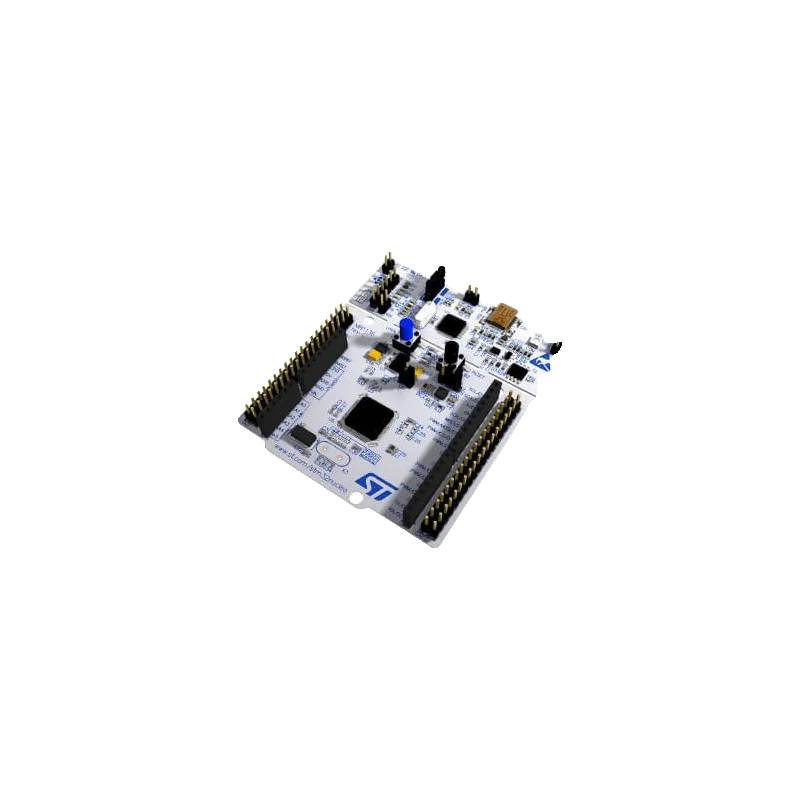
The Nucleo-F103RB is ST's Nucleo-64 board (MB1136) around an STM32F103RBT6, a 72 MHz Arm Cortex-M3 with 128 KB of flash and 20 KB of SRAM: the same chip family as the Blue Pill (ST DS5319, p. 1). The built-in ST-LINK/V2-1 programs it over mini-USB and carries Serial (USART2, PA2/PA3) as a virtual COM port; USB supplies 300 mA, VIN takes 7 V to 12 V (UM1724, pp. 20, 21, 25). Its Arduino headers run at 3.3 V, and its analog-capable pins, A0 to A5 among them, are not 5 V tolerant (DS5319, pp. 28 to 33).
The NUCLEO-F103RB puts ST's classic medium-density STM32F103 on the MB1136 Nucleo-64 board of UM1724: Arduino Uno V3 headers, two 38-pin ST morpho headers that carry every MCU pin, a blue USER button, a green LED, and a snap-off ST-LINK/V2-1 that programs over SWD and shows up as a USB drive and a COM port (UM1724, pp. 6, 16).
The STM32F103RB runs a Cortex-M3 at up to 72 MHz from 128 KB of flash and 20 KB of SRAM, with two 12-bit 1 µs ADCs (up to 16 channels), three USARTs, two SPI, two I2C, a CAN 2.0B controller and a full-speed USB device (DS5319, p. 1). There is no FPU and no DAC. It is a good board for following the many F103 tutorials written for the Blue Pill, with a programmer and debugger already on board.
The 5 V story differs from the newer Nucleos: almost all digital pins are 5 V tolerant, but every pin with an ADC input (PA0 to PA7, PB0, PB1, PC0 to PC5), plus PB5 and PC13 to PC15, is not (DS5319, pin table pp. 28 to 33). On the Arduino header that means A0 to A5, D4, D11 to D13 and D0/D1 must stay at 3.3 V.
Nucleo-F103RB pinout
| Pin | Function | Type |
|---|---|---|
| NC | NC (CN6 pin 1) | passive |
| IOREF | IOREF (CN6 pin 2)3.3 V | power out |
| RESET | RESET (CN6 pin 3)3.3 V | input |
| 3V3 | 3.3V (CN6 pin 4)3.3 V | power out |
| 5V | 5V (CN6 pin 5)5 V | power out |
| GND | GND (CN6 pin 6) | power in |
| GND-2 | GND (CN6 pin 7) | power in |
| VIN | VIN (CN6 pin 8)7 V to 12 V | power in |
| A0 | ADC1_IN0, ADC2_IN0, PWM TIM2_CH1, Digital3.3 V only (not 5 V tolerant) | bidirectional |
| A1 | ADC1_IN1, ADC2_IN1, PWM TIM2_CH2, Digital3.3 V only (not 5 V tolerant) | bidirectional |
| A2 | ADC1_IN4, ADC2_IN4, SPI1_NSS, Digital3.3 V only (not 5 V tolerant) | bidirectional |
| A3 | ADC1_IN8, ADC2_IN8, PWM TIM1_CH2N, PWM TIM3_CH3, Digital3.3 V only (not 5 V tolerant) | bidirectional |
| A4 | ADC1_IN11, ADC2_IN11, Digital3.3 V only (not 5 V tolerant) | bidirectional |
| A5 | ADC1_IN10, ADC2_IN10, Digital3.3 V only (not 5 V tolerant) | bidirectional |
| D15 | PWM TIM4_CH3, I2C1_SCL, CAN_RX, Digital3.3 V, 5 V tolerant as digital I/O | bidirectional |
| D14 | PWM TIM4_CH4, I2C1_SDA, CAN_TX, Digital3.3 V, 5 V tolerant as digital I/O | bidirectional |
| AREF | AREF3.3 V | power in |
| GND-3 | GND (CN5 pin 7) | power in |
| D13 | ADC1_IN5, ADC2_IN5, SPI1_SCK, Digital3.3 V only (not 5 V tolerant) | bidirectional |
| D12 | ADC1_IN6, ADC2_IN6, PWM TIM3_CH1, SPI1_MISO, Digital3.3 V only (not 5 V tolerant) | bidirectional |
| D11 | ADC1_IN7, ADC2_IN7, PWM TIM1_CH1N, PWM TIM3_CH2, SPI1_MOSI, Digital3.3 V only (not 5 V tolerant) | bidirectional |
| D10 | PWM TIM4_CH1, USART1_TX, I2C1_SCL, Digital3.3 V, 5 V tolerant as digital I/O | bidirectional |
| D9 | PWM TIM3_CH2, Digital3.3 V, 5 V tolerant as digital I/O | bidirectional |
| D8 | PWM TIM1_CH2, USART1_TX, Digital3.3 V, 5 V tolerant as digital I/O | bidirectional |
| D7 | PWM TIM1_CH1, Digital3.3 V, 5 V tolerant as digital I/O | bidirectional |
| D6 | PWM TIM2_CH3, USART3_TX, I2C2_SCL, Digital3.3 V, 5 V tolerant as digital I/O | bidirectional |
| D5 | PWM TIM3_CH1, SPI1_MISO, Digital3.3 V, 5 V tolerant as digital I/O | bidirectional |
| D4 | PWM TIM3_CH2, SPI1_MOSI, Digital3.3 V only (not 5 V tolerant) | bidirectional |
| D3 | PWM TIM2_CH2, SPI1_SCK, SWO, Digital3.3 V, 5 V tolerant as digital I/O | bidirectional |
| D2 | PWM TIM1_CH3, USART1_RX, Digital3.3 V, 5 V tolerant as digital I/O | bidirectional |
| D1 | ADC1_IN2, ADC2_IN2, PWM TIM2_CH3, USART2_TX, Digital3.3 V only (not 5 V tolerant) | bidirectional |
| D0 | ADC1_IN3, ADC2_IN3, PWM TIM2_CH4, USART2_RX, Digital3.3 V only (not 5 V tolerant) | bidirectional |
| PC10 | USART3_TX, Digital3.3 V, 5 V tolerant as digital I/O | bidirectional |
| PC11 | USART3_RX, Digital3.3 V, 5 V tolerant as digital I/O | bidirectional |
| PC12 | Digital3.3 V, 5 V tolerant as digital I/O | bidirectional |
| PD2 | Digital3.3 V, 5 V tolerant as digital I/O | bidirectional |
| E5V | E5V (CN7 pin 6)4.75 V to 5.25 V | power in |
| BOOT0 | BOOT0 (CN7 pin 7)3.3 V | input |
| PA13 | SWDIO, Digital3.3 V, 5 V tolerant as digital I/O | bidirectional |
| PA14 | SWCLK, Digital3.3 V, 5 V tolerant as digital I/O | bidirectional |
| PA15 | PWM TIM2_CH1, SPI1_NSS, Digital3.3 V, 5 V tolerant as digital I/O | bidirectional |
| PB7 | PWM TIM4_CH2, USART1_RX, I2C1_SDA, Digital3.3 V, 5 V tolerant as digital I/O | bidirectional |
| PC13 | Digital3.3 V only (not 5 V tolerant) | bidirectional |
| PC14 | LSE in, Digital3.3 V only (not 5 V tolerant) | bidirectional |
| PC15 | LSE out, Digital3.3 V only (not 5 V tolerant) | bidirectional |
| PD0 | HSE in, Digital3.3 V only (not 5 V tolerant) | bidirectional |
| PD1 | HSE out, Digital3.3 V only (not 5 V tolerant) | bidirectional |
| VBAT | VBAT (CN7 pin 33) | power in |
| PC2 | ADC1_IN12, ADC2_IN12, Digital3.3 V only (not 5 V tolerant) | bidirectional |
| PC3 | ADC1_IN13, ADC2_IN13, Digital3.3 V only (not 5 V tolerant) | bidirectional |
| PC9 | PWM TIM3_CH4, Digital3.3 V, 5 V tolerant as digital I/O | bidirectional |
| PC8 | PWM TIM3_CH3, Digital3.3 V, 5 V tolerant as digital I/O | bidirectional |
| PC6 | PWM TIM3_CH1, Digital3.3 V, 5 V tolerant as digital I/O | bidirectional |
| PC5 | ADC1_IN15, ADC2_IN15, Digital3.3 V only (not 5 V tolerant) | bidirectional |
| U5V | U5V (CN10 pin 8)5 V | power out |
| PA12 | CAN_TX, USB D+, Digital3.3 V, 5 V tolerant as digital I/O | bidirectional |
| PA11 | PWM TIM1_CH4, CAN_RX, USB D-, Digital3.3 V, 5 V tolerant as digital I/O | bidirectional |
| PB12 | SPI2_NSS, Digital3.3 V, 5 V tolerant as digital I/O | bidirectional |
| PB11 | PWM TIM2_CH4, USART3_RX, I2C2_SDA, Digital3.3 V, 5 V tolerant as digital I/O | bidirectional |
| PB2 | Digital3.3 V, 5 V tolerant as digital I/O | bidirectional |
| PB1 | ADC1_IN9, ADC2_IN9, PWM TIM1_CH3N, PWM TIM3_CH4, Digital3.3 V only (not 5 V tolerant) | bidirectional |
| PB15 | PWM TIM1_CH3N, SPI2_MOSI, Digital3.3 V, 5 V tolerant as digital I/O | bidirectional |
| PB14 | PWM TIM1_CH2N, SPI2_MISO, Digital3.3 V, 5 V tolerant as digital I/O | bidirectional |
| PB13 | PWM TIM1_CH1N, SPI2_SCK, Digital3.3 V, 5 V tolerant as digital I/O | bidirectional |
| AGND | AGND (CN10 pin 32) | power in |
| PC4 | ADC1_IN14, ADC2_IN14, Digital3.3 V only (not 5 V tolerant) | bidirectional |
Nucleo-F103RB code
Every example here compiles for its board.
// Nucleo-F103RB on Nucleo-F103RB: wiring and a free simulation at https://www.tinkered.ai/components/stm32-nucleo-f103rb
// Nucleo-F103RB: blink the user LED and read an analog input in millivolts.
// Serial is the ST-LINK virtual COM port: open it at 115200 baud.
// The ADC reference is measured from the chip's internal reference (AVREF),
// so the reading stays right whatever voltage feeds VREF+.
#include "stm32yyxx_ll_adc.h"

const int LED_PIN = LED_BUILTIN;   // D13 (PA5), the green LD2
const int ANALOG_PIN = A0;          // PA0 on the Arduino header; 0 to 3.3 V only, PA0 is not 5 V tolerant
const uint32_t VREFINT_TYP_MV = 1200;  // typical internal reference, used only if no calibration value exists

uint32_t readVrefMv() {
#if defined(AVREF)
  uint32_t raw = analogRead(AVREF);
  if (raw == 0) return 3300;
#if defined(__LL_ADC_CALC_VREFANALOG_VOLTAGE)
  return __LL_ADC_CALC_VREFANALOG_VOLTAGE(raw, LL_ADC_RESOLUTION_12B);
#else
  return VREFINT_TYP_MV * 4095UL / raw;
#endif
#else
  return 3300;
#endif
}

void setup() {
  pinMode(LED_PIN, OUTPUT);
  analogReadResolution(12);        // 0 to 4095
  Serial.begin(115200);
}

void loop() {
  static bool ledOn = false;
  ledOn = !ledOn;
  digitalWrite(LED_PIN, ledOn ? HIGH : LOW);

  uint32_t vrefMv = readVrefMv();
  uint32_t raw = analogRead(ANALOG_PIN);
  uint32_t millivolts = raw * vrefMv / 4095;
  Serial.print("VREF+ ");
  Serial.print(vrefMv);
  Serial.print(" mV   A0 raw=");
  Serial.print(raw);
  Serial.print("  ");
  Serial.print(millivolts);
  Serial.println(" mV");

  delay(500);
}
Before you wire it
- Keep 5 V signals on FT pins used as digital inputs; A0 to A5, D11 to D13, D4 and D0/D1 are not 5 V tolerant on the F103 (DS5319, pp. 28 to 33).
- Keep both CN2 jumpers on to program the target with the on-board ST-LINK (UM1724, p. 16).
- Use D14 (PB9) and D15 (PB8) for I2C, and Serial1 on D8 (PA9) and D2 (PA10) for a serial module (UM1724, pp. 25, 39).
- Switch to VIN or E5V when the board and its shields need more than 300 mA, powering it before plugging in USB (UM1724, pp. 20, 22).
- Never put more than 3.6 V on an analog pin or on PA0 to PA7, PB0, PB1 or PC0 to PC5 (DS5319, pp. 1, 28 to 33).
- Never source current from PC13 to PC15: they sit behind the backup power switch, which sinks only 3 mA, and must not drive an LED (DS5319, p. 33, note 5).
- Never use PA13/PA14 while the ST-LINK is attached; they carry SWD (UM1724, p. 55).
- Serial (USART2 on PA2/PA3) goes to the ST-LINK through SB13/SB14, so D0/D1 are open as shipped; closing SB62/SB63 and opening SB13/SB14 moves it to the header (UM1724, p. 25). USART3 on PC10/PC11 can then be wired to the ST-LINK's CN3 with two flying wires.
- In LQFP64 the F103's HSE pins are PD0/PD1. MB1136 C-02 and later boards feed PD0 from the ST-LINK's fixed 8 MHz MCO (UM1724, p. 24).
- PB2 is also BOOT1, read with BOOT0 at reset; leave it low at power-up unless you mean to boot from SRAM.
- USB on PA11/PA12 shares those pins with CAN on the F103 (DS5319 pin table), so the two can't run at the same time.
- D13 is both SPI1 SCK and the LD2 LED (UM1724, pp. 23, 39).
Specifications
- Microcontroller
- STM32F103RBT6, Arm Cortex-M3, up to 72 MHzST STM32F103x8/xB datasheet DS5319 Rev 18, p. 1
- Memory
- 128 KB flash, 20 KB SRAMST STM32F103x8/xB datasheet DS5319 Rev 18, p. 1
- I/O voltage
- 2.0 V to 3.6 V supply, 3.3 V on the board; FT pins tolerate 5 V, ADC-capable pins, PB5 and PC13 to PC15 do notST STM32F103x8/xB datasheet DS5319 Rev 18, pp. 1, 28 to 33
- Current
- 25 mA per pin, 150 mA in total into VDDST STM32F103x8/xB datasheet DS5319 Rev 18, p. 37
- ADC
- Two 12-bit 1 µs ADCs, up to 16 channels, 0 to 3.6 V range; no DACST STM32F103x8/xB datasheet DS5319 Rev 18, p. 1
- Interfaces
- 3 USART, 2 SPI, 2 I2C, CAN 2.0B, USB 2.0 full-speed deviceST STM32F103x8/xB datasheet DS5319 Rev 18, p. 1
- Programmer and USB
- ST-LINK/V2-1 on mini-USB: SWD, USB drive and virtual COM port on USART2 (PA2/PA3)ST UM1724 (STM32 Nucleo-64 boards MB1136), Rev 14, pp. 6, 16, 25
- Power inputs
- USB (300 mA after enumeration), VIN 7 V to 12 V, E5V 4.75 V to 5.25 V, or 3.3 VST UM1724 (STM32 Nucleo-64 boards MB1136), Rev 14, pp. 20 to 22
- 3.3 V output
- Regulator U4, 500 mA maximumST UM1724 (STM32 Nucleo-64 boards MB1136), Rev 14, p. 22
- User LED and button
- LD2 green on D13 (PA5), HIGH = on; B1 USER on PC13ST UM1724 (STM32 Nucleo-64 boards MB1136), Rev 14, p. 23
From the UM1724 STM32 Nucleo-64 boards (MB1136) user manual, published by STMicroelectronics.
Common mistakes
Driving a 5 V sensor into an analog pin
On the F103 the ADC pins are not 5 V tolerant at all, even as digital inputs (DS5319, pp. 28 to 33). A 5 V output on A0 to A5 needs a divider or a level shifter.
Wiring a module to D0/D1 for Serial
USART2 belongs to the ST-LINK as shipped, so nothing reaches D0/D1 (UM1724, p. 25). Use Serial1 on D8/D2 or move the solder bridges.
Looking for I2C on A4/A5
A4/A5 are PC1/PC0 analog inputs by default; I2C1 is on D14/D15 (PB9/PB8) (UM1724, p. 39).
Expecting floating-point speed
The Cortex-M3 has no FPU, so float maths runs in software and is far slower than on an F4 or G4 Nucleo. Use integer maths in tight loops.
Nucleo-F103RB questions
Nucleo-F103RB vs Blue Pill: what is the difference?
Both use an STM32F103 at 72 MHz with 20 KB of SRAM; the Nucleo's F103RB has 128 KB of flash and 51 I/Os against the Blue Pill's 64 KB and 37 (DS5319, p. 1). The Nucleo adds a built-in ST-LINK, Arduino and morpho headers and a regulator good for 500 mA (UM1724, p. 22), while the Blue Pill needs an external programmer.
Is the Nucleo-F103RB 5 V tolerant?
Partly. FT pins accept 5 V as digital inputs, but every ADC-capable pin (PA0 to PA7, PB0, PB1, PC0 to PC5), PB5 and PC13 to PC15 are limited to 3.6 V (DS5319, pp. 28 to 33). On the Arduino header that rules out A0 to A5, D0, D1, D4 and D11 to D13.
Where is Serial on the Nucleo-F103RB?
Serial is USART2 on PA2/PA3, connected to the ST-LINK as a virtual COM port over the mini-USB cable (UM1724, p. 25). D0/D1 are disconnected unless you swap SB13/SB14 for SB62/SB63.
Can the Nucleo-F103RB use CAN or USB?
The STM32F103RB has both a CAN 2.0B controller and a full-speed USB device, on the same PA11/PA12 pins (DS5319, p. 1 and pin table). The board brings them to the morpho header only, so you add a CAN transceiver or a USB connector yourself.
How do I upload to the Nucleo-F103RB?
Install the STM32duino core, pick Nucleo-64 and the F103RB, and upload over the ST-LINK by Mass Storage or STM32CubeProgrammer. On Windows 7 and 8, install the ST-LINK/V2-1 driver before plugging the board in (UM1724, p. 17).
Build something with the Nucleo-F103RB
- Build this
CAN bus sniffer
Read a CAN bus with the F103's own controller and a transceiver.
- Build this
Learning STM32 registers
Blink LD2 and read B1 with direct register access in STM32CubeIDE.
- Build this
Shield data logger
Log analog readings to an SD card shield on the Arduino headers.
This page as plain Markdown, for ChatGPT, Claude or your own agent. /components/stm32-nucleo-f103rb.md