STM32 Nucleo-F401RE
ST's Uno-shaped STM32 board: an 84 MHz Cortex-M4F with 512 KB of flash and a built-in ST-LINK programmer on one USB cable.
- MicrocontrollerSTM32F401RET6, Arm Cortex-M4 with FPU, up to 84 MHz
- Memory512 KB flash, 96 KB SRAM
- Chip supply and I/O1.7 V to 3.6 V; I/O ports 5 V tolerant
- GPIO and ADC (LQFP64)50 GPIOs; one 12-bit 2.4 MSPS ADC, 16 channels
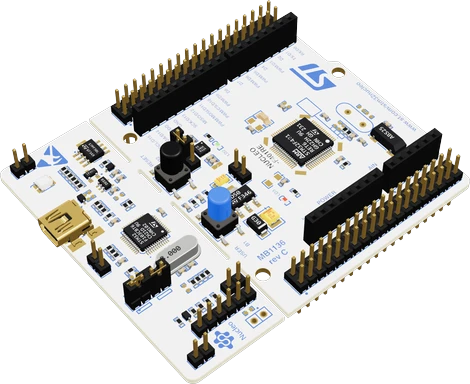
The Nucleo-F401RE is ST's Nucleo-64 board around an STM32F401RET6, an Arm Cortex-M4F at up to 84 MHz with 512 KB of flash and 96 KB of SRAM (STM32F401xD/xE datasheet, p. 1). Plug its mini-USB into a computer to power it, flash it through the on-board ST-LINK/V2-1 and open Serial (USART2 on PA2/PA3) as a virtual COM port, or feed 7 V to 12 V into VIN (UM1724, pp. 16, 21, 25). Wire shields to the Arduino Uno headers at 3.3 V logic: I2C is D14/D15 (PB9/PB8), the green LD2 is D13 (PA5) and the blue user button is PC13 (UM1724, pp. 23, 43).
The NUCLEO-F401RE is one of ST's Nucleo-64 development boards, all built on the MB1136 reference board and documented in the UM1724 user manual. It carries an STM32F401RET6 in an LQFP64 package and splits into two parts: the target half with the microcontroller, its headers, buttons and LEDs, and a snap-off ST-LINK/V2-1 half that programs, debugs and powers it over a single mini-USB cable (UM1724, pp. 15, 16).
The chip is a Cortex-M4 with a floating-point unit and DSP instructions, running at up to 84 MHz from 512 KB of flash and 96 KB of SRAM. In the LQFP64 package it gives 50 GPIOs, a 12-bit 2.4 MSPS ADC on up to 16 channels, three USARTs, SPI with two I2S-capable ports, an SDIO card interface and a USB 2.0 full-speed OTG controller (STM32F401xD/xE datasheet, pp. 1, 11). It has no DAC and no CAN controller.
On the board, the Arduino Uno V3 headers carry the familiar D0 to D15 and A0 to A5 names, and the two ST morpho headers bring out every MCU pin. A few details differ from an Uno and catch people out: Serial is USART2, routed to the ST-LINK's virtual COM port rather than to D0/D1 as shipped, A4/A5 are PC1/PC0 rather than the I2C pins, and the board's logic level is 3.3 V (UM1724, pp. 25, 43). It is programmed from STM32CubeIDE, the Arduino IDE with the STM32duino core, PlatformIO or Mbed.
STM32 Nucleo-F401RE pinout
| Pin | Function | Type |
|---|---|---|
| IOREF | IOREF (3.3 V) | power out |
| NRST | RESET (NRST) | input |
| 3V3 | +3.3V3.3 V | power out |
| 5V | +5V5 V | power out |
| GND | GND | power in |
| GND_2 | GND | power in |
| VIN | VIN (7-12 V) | power in |
| A0 | Digital, ADC1_IN0, PWM, UART USART2 CTS3.3 V, 5 V tolerant | bidirectional |
| A1 | Digital, ADC1_IN1, PWM, UART USART2 RTS3.3 V, 5 V tolerant | bidirectional |
| A2 | Digital, ADC1_IN4, I2S I2S3 WS, SPI1 NSS, SPI3 NSS3.3 V, 5 V tolerant | bidirectional |
| A3 | Digital, ADC1_IN8, PWM3.3 V, 5 V tolerant | bidirectional |
| A4 | Digital, ADC1_IN113.3 V, 5 V tolerant | bidirectional |
| A5 | Digital, ADC1_IN103.3 V, 5 V tolerant | bidirectional |
| D8 | Digital, PWM, UART USART1 TX3.3 V, 5 V tolerant | bidirectional |
| D9 | Digital, I2S I2S3 MCK, SDIO SDIO D7, PWM, UART USART6 RX3.3 V, 5 V tolerant | bidirectional |
| D10 | Digital, I2C1 SCL, PWM, UART USART1 TX3.3 V, 5 V tolerant | bidirectional |
| D11 | Digital, ADC1_IN7, SPI1 MOSI, PWM3.3 V, 5 V tolerant | bidirectional |
| D12 | Digital, ADC1_IN6, SPI1 MISO, PWM3.3 V, 5 V tolerant | bidirectional |
| D13 | Digital, ADC1_IN5, SPI1 SCK, PWM3.3 V, 5 V tolerant | bidirectional |
| GND_3 | GND | power in |
| AREF | AREF (AVDD) | power out |
| D14 | Digital, I2C1 SDA, I2S I2S2 WS, SDIO SDIO D5, SPI2 NSS, PWM3.3 V, 5 V tolerant | bidirectional |
| D15 | Digital, I2C1 SCL, SDIO SDIO D4, PWM3.3 V, 5 V tolerant | bidirectional |
| D0 | D0 (not connected: PA3 through SB62, open as shipped) | bidirectional |
| D1 | D1 (not connected: PA2 through SB63, open as shipped) | bidirectional |
| D2 | Digital, PWM, UART USART1 RX3.3 V, 5 V tolerant | bidirectional |
| D3 | Digital, I2C2 SDA, I2S I2S3 CK, SPI1 SCK, SPI3 SCK, PWM3.3 V, 5 V tolerant | bidirectional |
| D4 | Digital, I2S I2S3 SD, SPI1 MOSI, SPI3 MOSI, PWM3.3 V, 5 V tolerant | bidirectional |
| D5 | Digital, I2C3 SDA, SPI1 MISO, SPI3 MISO, PWM3.3 V, 5 V tolerant | bidirectional |
| D6 | Digital, I2C2 SCL, I2S I2S2 CK, SPI2 SCK, PWM3.3 V, 5 V tolerant | bidirectional |
| D7 | Digital, I2C3 SCL, PWM3.3 V, 5 V tolerant | bidirectional |
| CN7_1 | Digital, I2S I2S3 CK, SDIO SDIO D2, SPI3 SCK3.3 V, 5 V tolerant | bidirectional |
| CN7_2 | Digital, SDIO SDIO D3, SPI3 MISO3.3 V, 5 V tolerant | bidirectional |
| CN7_3 | Digital, I2S I2S3 SD, SDIO SDIO CK, SPI3 MOSI3.3 V, 5 V tolerant | bidirectional |
| CN7_4 | Digital, SDIO SDIO CMD3.3 V, 5 V tolerant | bidirectional |
| CN7_5 | CN7-5 (VDD) | power out |
| CN7_6 | CN7-6 (E5V) | power in |
| CN7_7 | strapping | input |
| CN7_8 | CN7-8 (GND) | power in |
| CN7_9 | CN7-9 (NC) | no connect |
| CN7_10 | CN7-10 (NC) | no connect |
| CN7_11 | CN7-11 (NC) | no connect |
| CN7_12 | CN7-12 (IOREF) | power out |
| CN7_13 | Digital3.3 V, 5 V tolerant | bidirectional |
| CN7_14 | Digital3.3 V | input |
| CN7_15 | Digital3.3 V, 5 V tolerant | bidirectional |
| CN7_16 | CN7-16 (+3.3V) | power out |
| CN7_17 | Digital, I2S I2S3 WS, SPI1 NSS, SPI3 NSS, PWM3.3 V, 5 V tolerant | bidirectional |
| CN7_18 | CN7-18 (+5V) | power out |
| CN7_19 | CN7-19 (GND) | power in |
| CN7_20 | CN7-20 (GND) | power in |
| CN7_21 | Digital, I2C1 SDA, PWM, UART USART1 RX3.3 V, 5 V tolerant | bidirectional |
| CN7_22 | CN7-22 (GND) | power in |
| CN7_23 | Digital3.3 V, 5 V tolerant | bidirectional |
| CN7_24 | CN7-24 (VIN) | power in |
| CN7_25 | Digital3.3 V, 5 V tolerant | bidirectional |
| CN7_26 | CN7-26 (NC) | no connect |
| CN7_27 | Digital3.3 V, 5 V tolerant | bidirectional |
| CN7_28 | Digital, ADC1_IN0, PWM, UART USART2 CTS3.3 V, 5 V tolerant | bidirectional |
| CN7_29 | Digital3.3 V, 5 V tolerant | bidirectional |
| CN7_30 | Digital, ADC1_IN1, PWM, UART USART2 RTS3.3 V, 5 V tolerant | bidirectional |
| CN7_31 | Digital3.3 V, 5 V tolerant | bidirectional |
| CN7_32 | Digital, ADC1_IN4, I2S I2S3 WS, SPI1 NSS, SPI3 NSS3.3 V, 5 V tolerant | bidirectional |
| CN7_33 | CN7-33 (VBAT) | power in |
| CN7_34 | Digital, ADC1_IN8, PWM3.3 V, 5 V tolerant | bidirectional |
| CN7_35 | Digital, ADC1_IN12, SPI2 MISO3.3 V, 5 V tolerant | bidirectional |
| CN7_36 | Digital, ADC1_IN113.3 V, 5 V tolerant | bidirectional |
| CN7_37 | Digital, ADC1_IN13, I2S I2S2 SD, SPI2 MOSI3.3 V, 5 V tolerant | bidirectional |
| CN7_38 | Digital, ADC1_IN103.3 V, 5 V tolerant | bidirectional |
| CN10_1 | Digital, I2C3 SDA, SDIO SDIO D1, PWM3.3 V, 5 V tolerant | bidirectional |
| CN10_2 | Digital, SDIO SDIO D0, PWM3.3 V, 5 V tolerant | bidirectional |
| CN10_3 | Digital, I2C1 SCL, SDIO SDIO D4, PWM3.3 V, 5 V tolerant | bidirectional |
| CN10_4 | Digital, I2S I2S2 MCK, SDIO SDIO D6, PWM, UART USART6 TX3.3 V, 5 V tolerant | bidirectional |
| CN10_5 | Digital, I2C1 SDA, I2S I2S2 WS, SDIO SDIO D5, SPI2 NSS, PWM3.3 V, 5 V tolerant | bidirectional |
| CN10_6 | Digital, ADC1_IN153.3 V, 5 V tolerant | bidirectional |
| CN10_7 | CN10-7 (AVDD) | power out |
| CN10_8 | CN10-8 (U5V) | power in |
| CN10_9 | CN10-9 (GND) | power in |
| CN10_10 | CN10-10 (NC) | no connect |
| CN10_11 | Digital, ADC1_IN5, SPI1 SCK, PWM3.3 V, 5 V tolerant | bidirectional |
| CN10_12 | Digital, UART USART1 RTS, UART USART6 RX, USB USB D+3.3 V, 5 V tolerant | bidirectional |
| CN10_13 | Digital, ADC1_IN6, SPI1 MISO, PWM3.3 V, 5 V tolerant | bidirectional |
| CN10_14 | Digital, PWM, UART USART1 CTS, UART USART6 TX, USB USB D-3.3 V, 5 V tolerant | bidirectional |
| CN10_15 | Digital, ADC1_IN7, SPI1 MOSI, PWM3.3 V, 5 V tolerant | bidirectional |
| CN10_16 | Digital, I2S I2S2 WS, SPI2 NSS3.3 V, 5 V tolerant | bidirectional |
| CN10_17 | Digital, I2C1 SCL, PWM, UART USART1 TX3.3 V, 5 V tolerant | bidirectional |
| CN10_18 | CN10-18 (NC) | no connect |
| CN10_19 | Digital, I2S I2S3 MCK, SDIO SDIO D7, PWM, UART USART6 RX3.3 V, 5 V tolerant | bidirectional |
| CN10_20 | CN10-20 (GND) | power in |
| CN10_21 | Digital, PWM, UART USART1 TX3.3 V, 5 V tolerant | bidirectional |
| CN10_22 | Digital3.3 V, 5 V tolerant | bidirectional |
| CN10_23 | Digital, I2C3 SCL, PWM3.3 V, 5 V tolerant | bidirectional |
| CN10_24 | Digital, ADC1_IN9, PWM3.3 V, 5 V tolerant | bidirectional |
| CN10_25 | Digital, I2C2 SCL, I2S I2S2 CK, SPI2 SCK, PWM3.3 V, 5 V tolerant | bidirectional |
| CN10_26 | Digital, I2S I2S2 SD, SPI2 MOSI, PWM3.3 V, 5 V tolerant | bidirectional |
| CN10_27 | Digital, I2C3 SDA, SPI1 MISO, SPI3 MISO, PWM3.3 V, 5 V tolerant | bidirectional |
| CN10_28 | Digital, SPI2 MISO, PWM3.3 V, 5 V tolerant | bidirectional |
| CN10_29 | Digital, I2S I2S3 SD, SPI1 MOSI, SPI3 MOSI, PWM3.3 V, 5 V tolerant | bidirectional |
| CN10_30 | Digital, I2S I2S2 CK, SPI2 SCK, PWM3.3 V, 5 V tolerant | bidirectional |
| CN10_31 | Digital, I2C2 SDA, I2S I2S3 CK, SPI1 SCK, SPI3 SCK, PWM3.3 V, 5 V tolerant | bidirectional |
| CN10_32 | CN10-32 (AGND) | power in |
| CN10_33 | Digital, PWM, UART USART1 RX3.3 V, 5 V tolerant | bidirectional |
| CN10_34 | Digital, ADC1_IN143.3 V, 5 V tolerant | bidirectional |
| CN10_35 | Digital, ADC1_IN2, PWM, UART USART2 TX3.3 V, 5 V tolerant | bidirectional |
| CN10_36 | CN10-36 (NC) | no connect |
| CN10_37 | Digital, ADC1_IN3, PWM, UART USART2 RX3.3 V, 5 V tolerant | bidirectional |
| CN10_38 | CN10-38 (NC) | no connect |
Specifications
- Microcontroller
- STM32F401RET6, Arm Cortex-M4 with FPU, up to 84 MHzSTM32F401xD/xE datasheet (DocID025644 Rev 3), p. 1
- Memory
- 512 KB flash, 96 KB SRAMSTM32F401xD/xE datasheet, p. 1
- Chip supply and I/O
- 1.7 V to 3.6 V; I/O ports 5 V tolerantSTM32F401xD/xE datasheet, p. 1
- GPIO and ADC (LQFP64)
- 50 GPIOs; one 12-bit 2.4 MSPS ADC, 16 channelsSTM32F401xD/xE datasheet, pp. 1, 11
- Board power inputs
- USB (U5V), VIN 7 V to 12 V, E5V 4.75 V to 5.25 V, or +3.3V 3 V to 3.6 VUM1724 Rev 14, pp. 19, 21, 22
- VIN input current
- 800 mA at 7 V, 450 mA up to 9 V, 250 mA up to 12 VUM1724 Rev 14, p. 21
- Current over USB
- 300 mA for the whole board and shields after enumerationUM1724 Rev 14, pp. 19, 20
- 3.3 V output
- Limited by regulator U4, 500 mA maxUM1724 Rev 14, p. 22
- On-board programmer
- ST-LINK/V2-1 (SWD), mini-USB, virtual COM port on USART2 (PA2/PA3)UM1724 Rev 14, pp. 16, 25
- User LED and button
- LD2 green on D13 (PA5), lit HIGH; B1 USER on PC13; B2 RESET on NRSTUM1724 Rev 14, p. 23
- Logic level
- 3.3 V
- Clock speed
- 84 MHz
- Flash
- 512 KB
- RAM
- 96 KB
- GPIO pins
- 50
- ADC channels
- 16
- ADC resolution
- 12 bits
- PWM channels
- 17
- Dimensions
- 82.5 × 20.3 × 70 mm
- Weight
- 37 g
From the STMicroelectronics's datasheet, published by STMicroelectronics.
Common mistakes
Wiring a module to D0/D1 for Serial
As shipped, D0/D1 are not connected: USART2 goes to the ST-LINK's virtual COM port through SB13/SB14, with SB62/SB63 open (UM1724, p. 25). Use USART1 on D8/D2, or move the solder bridges.
Looking for I2C on A4/A5
On the Nucleo, A4 and A5 are PC1 and PC0, analog inputs. I2C1 is on D14 (PB9, SDA) and D15 (PB8, SCL), the pins next to AREF (UM1724, p. 43).
Drawing more than 300 mA from USB
Over USB the board and its shields get 300 mA at most; past that, ST asks you to power it from VIN or E5V (UM1724, p. 20). Motors, servos and LED strips need their own supply with a shared ground.
Powering it from a USB phone charger
A charger does not enumerate the board, so LD3 stays off and the STM32 is not powered. Fit jumper JP1 to power the target anyway (UM1724, p. 20).
Expecting analogWrite to give a voltage
The STM32F401 has no DAC, so analogWrite is PWM on a timer pin. For a true analog output, use the Nucleo-F446RE or Nucleo-L476RG, whose chips have 12-bit DACs on PA4 and PA5.
STM32 Nucleo-F401RE questions
Is the Nucleo-F401RE 5 V or 3.3 V?
3.3 V. The board's IOREF and logic run at 3.3 V, although it has a +5V pin for shields (UM1724, p. 22). ST rates the STM32F401's I/O ports 5 V tolerant (datasheet, p. 1), so 5 V digital inputs are accepted, but outputs only reach 3.3 V and the ADC reads 0 to 3.3 V.
Why won't my Nucleo-F401RE upload or show up on the computer?
Check that both CN2 jumpers are on, the default that lets the ST-LINK program the on-board chip (UM1724, p. 16), and that the mini-USB cable carries data. On Windows, install the ST-LINK/V2-1 driver first; if the board was plugged in before, Device Manager shows Unknown devices to update by hand (p. 17). LD1 blinks red then turns green as the ST-LINK talks to the target, and orange means a communication failure (p. 23).
Where is Serial on the Nucleo-F401RE?
Serial is USART2 on PA2/PA3, wired to the ST-LINK, so it appears on the computer as a virtual COM port over the same USB cable (UM1724, p. 25). It is not on D0/D1 unless you close SB62/SB63 and open SB13/SB14.
How do I power the Nucleo-F401RE without USB?
Feed 7 V to 12 V into VIN (CN6 pin 8 or CN7 pin 24), or a regulated 4.75 V to 5.25 V into E5V, with JP5 moved to E5V and JP1 removed (UM1724, p. 21). VIN can supply up to 800 mA at 7 V, less as the voltage rises.
Which pin is the built-in LED on the Nucleo-F401RE?
LD2, the green user LED, is on D13, which is PA5 on this board; HIGH turns it on (UM1724, p. 23). The blue B1 USER button is PC13, and B2 RESET is NRST.
Nucleo-F401RE vs Nucleo-F446RE: which should I buy?
Both share the same Nucleo-64 board and headers. The F401RE runs at 84 MHz with 96 KB of SRAM (F401 datasheet, p. 1); the F446RE runs at 180 MHz with 128 KB of SRAM and adds two 12-bit DACs and two CAN controllers (F446 datasheet, p. 1). Pick the F446RE for audio, CAN or heavy DSP, the F401RE for general projects.
Do I need a separate programmer like a Blue Pill does?
No. The Nucleo carries an ST-LINK/V2-1 on its snap-off end that flashes and debugs the STM32 over SWD from the same USB cable (UM1724, p. 16). It also mounts as a USB drive, so a compiled.bin can be copied onto it.
Build something with the STM32 Nucleo-F401RE
- Build this
Learning STM32 with STM32CubeIDE
Blink LD2, read B1 and print to the virtual COM port while stepping through code in the built-in ST-LINK debugger.
- Build this
Arduino shield projects at 3.3 V
Stack an Arduino-format motor, display or sensor shield on the Uno headers and drive it from the faster Cortex-M4F.
- Build this
SD card data logger
Log sensor readings to a microSD card through the F401's SDIO interface or an SPI card module.
- Build this
I2S audio playback or capture
Drive an I2S amplifier such as a MAX98357A or read an I2S microphone from the F401's I2S-capable SPI ports.
- Build this
Motor and robot controller
Use the hardware timers for PWM and quadrature encoder inputs on a small robot or a closed-loop motor test rig.
This page as plain Markdown, for ChatGPT, Claude or your own agent. /components/stm32-nucleo-f401re.md