STM32 Nucleo-L476RG
ST's ultra-low-power Nucleo-64: an 80 MHz Cortex-M4F with 1 MB of flash that sleeps at 1.1 µA in Stop 2, with an on-board ST-LINK.
- MicrocontrollerSTM32L476RGT6, Arm Cortex-M4 with FPU, up to 80 MHz
- Memory1 MB flash in 2 banks, 128 KB SRAM (32 KB with parity)
- Chip supply1.71 V to 3.6 V
- Low-power figures100 µA/MHz run (LDO), 1.1 µA Stop 2, 120 nA Standby, 30 nA Shutdown
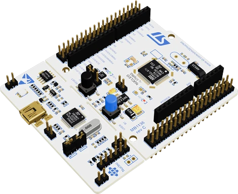
The Nucleo-L476RG is ST's Nucleo-64 board around an STM32L476RGT6, an ultra-low-power Arm Cortex-M4F at up to 80 MHz with 1 MB of flash, 128 KB of SRAM and a Stop 2 mode drawing 1.1 µA (STM32L476xx datasheet, p. 1). Power and program it through the mini-USB of its on-board ST-LINK/V2-1, which also carries Serial (USART2) as a virtual COM port, or feed 7 V to 12 V into VIN (UM1724, pp. 16, 21, 25). The Arduino Uno headers run at 3.3 V: I2C on D14/D15 (PB9/PB8), LD2 on D13 (PA5) and the user button on PC13 (UM1724, pp. 23, 52).
The NUCLEO-L476RG puts ST's STM32L4 ultra-low-power line on the standard Nucleo-64 board (MB1136, documented in UM1724). An STM32L476RGT6 in LQFP64 sits on the target half with its Arduino Uno V3 and ST morpho headers, LEDs and buttons; a snap-off ST-LINK/V2-1 on the other end programs, debugs and powers it over one mini-USB cable (UM1724, pp. 15, 16).
The STM32L476 runs a Cortex-M4 with FPU at up to 80 MHz from 1 MB of dual-bank flash and 128 KB of SRAM, 32 KB of it with hardware parity. Its strength is power: 100 µA/MHz in run mode on its LDO, 1.1 µA in Stop 2, 120 nA in Standby and 30 nA in Shutdown. It also brings a rich analog set, three 12-bit 5 MSPS ADCs, two 12-bit DAC channels, two op-amps and two comparators, plus one CAN controller, two SAI audio interfaces and USB OTG full speed (STM32L476xx datasheet, pp. 1, 2).
On the board, the L476RG's ST-LINK clock output is left unconnected to the MCU to keep low-power measurements clean, so the chip runs from its internal oscillators and the 32.768 kHz LSE crystal (UM1724, p. 25). Jumper JP6 (IDD) lets you put an ammeter in series with the MCU's supply to measure its current alone (p. 23). Serial, I2C and the LED sit where they do on every Nucleo-64: USART2 to the virtual COM port, I2C1 on D14/D15, LD2 on D13.
STM32 Nucleo-L476RG pinout
| Pin | Function | Type |
|---|---|---|
| IOREF | IOREF (3.3 V) | power out |
| NRST | RESET (NRST) | input |
| 3V3 | +3.3V3.3 V | power out |
| 5V | +5V5 V | power out |
| GND | GND | power in |
| GND_2 | GND | power in |
| VIN | VIN (7-12 V) | power in |
| A0 | Digital, ADC12_IN5, PWM, UART4 TX, UART USART2 CTS3.3 V | bidirectional |
| A1 | Digital, ADC12_IN6, PWM, UART4 RX, UART USART2 RTS3.3 V | bidirectional |
| A2 | Digital, ADC12_IN9, DAC DAC1 OUT1, SPI1 NSS, SPI3 NSS3.3 V | bidirectional |
| A3 | Digital, ADC12_IN15, PWM3.3 V | bidirectional |
| A4 | Digital, ADC123_IN2, I2C3 SDA, UART LPUART1 TX3.3 V | bidirectional |
| A5 | Digital, ADC123_IN1, I2C3 SCL, UART LPUART1 RX3.3 V | bidirectional |
| D8 | Digital, PWM, UART USART1 TX3.3 V | bidirectional |
| D9 | Digital, SDIO SDMMC1 D7, PWM3.3 V | bidirectional |
| D10 | Digital, I2C1 SCL, PWM, UART USART1 TX3.3 V | bidirectional |
| D11 | Digital, ADC12_IN12, SPI1 MOSI, PWM3.3 V | bidirectional |
| D12 | Digital, ADC12_IN11, SPI1 MISO, PWM, UART USART3 CTS3.3 V | bidirectional |
| D13 | Digital, ADC12_IN10, DAC DAC1 OUT2, SPI1 SCK, PWM3.3 V | bidirectional |
| GND_3 | GND | power in |
| AREF | AREF (AVDD) | power out |
| D14 | Digital, CAN CAN1 TX, I2C1 SDA, SDIO SDMMC1 D5, SPI2 NSS, PWM3.3 V | bidirectional |
| D15 | Digital, CAN CAN1 RX, I2C1 SCL, SDIO SDMMC1 D4, PWM3.3 V | bidirectional |
| D0 | D0 (not connected: PA3 through SB62, open as shipped) | bidirectional |
| D1 | D1 (not connected: PA2 through SB63, open as shipped) | bidirectional |
| D2 | Digital, PWM, UART USART1 RX3.3 V | bidirectional |
| D3 | Digital, SPI1 SCK, SPI3 SCK, PWM, UART USART1 RTS3.3 V | bidirectional |
| D4 | Digital, SPI1 MOSI, SPI3 MOSI, PWM, UART5 CTS3.3 V | bidirectional |
| D5 | Digital, SPI1 MISO, SPI3 MISO, PWM, UART5 RTS, UART USART1 CTS3.3 V | bidirectional |
| D6 | Digital, I2C2 SCL, UART LPUART1 RX, SPI2 SCK, PWM, UART USART3 TX3.3 V | bidirectional |
| D7 | Digital, PWM3.3 V | bidirectional |
| CN7_1 | Digital, SDIO SDMMC1 D2, SPI3 SCK, UART4 TX, UART USART3 TX3.3 V | bidirectional |
| CN7_2 | Digital, SDIO SDMMC1 D3, SPI3 MISO, UART4 RX, UART USART3 RX3.3 V | bidirectional |
| CN7_3 | Digital, SDIO SDMMC1 CK, SPI3 MOSI, UART5 TX3.3 V | bidirectional |
| CN7_4 | Digital, SDIO SDMMC1 CMD, UART5 RX, UART USART3 RTS3.3 V | bidirectional |
| CN7_5 | CN7-5 (VDD) | power out |
| CN7_6 | CN7-6 (E5V) | power in |
| CN7_7 | strapping | input |
| CN7_8 | CN7-8 (GND) | power in |
| CN7_9 | CN7-9 (NC) | no connect |
| CN7_10 | CN7-10 (NC) | no connect |
| CN7_11 | CN7-11 (NC) | no connect |
| CN7_12 | CN7-12 (IOREF) | power out |
| CN7_13 | Digital3.3 V | bidirectional |
| CN7_14 | Digital3.3 V | input |
| CN7_15 | Digital3.3 V | bidirectional |
| CN7_16 | CN7-16 (+3.3V) | power out |
| CN7_17 | Digital, SPI1 NSS, SPI3 NSS, PWM, UART4 RTS3.3 V | bidirectional |
| CN7_18 | CN7-18 (+5V) | power out |
| CN7_19 | CN7-19 (GND) | power in |
| CN7_20 | CN7-20 (GND) | power in |
| CN7_21 | Digital, I2C1 SDA, PWM, UART4 CTS, UART USART1 RX3.3 V | bidirectional |
| CN7_22 | CN7-22 (GND) | power in |
| CN7_23 | Digital3.3 V | bidirectional |
| CN7_24 | CN7-24 (VIN) | power in |
| CN7_25 | Digital3.3 V | bidirectional |
| CN7_26 | CN7-26 (NC) | no connect |
| CN7_27 | Digital3.3 V | bidirectional |
| CN7_28 | Digital, ADC12_IN5, PWM, UART4 TX, UART USART2 CTS3.3 V | bidirectional |
| CN7_29 | Digital3.3 V | bidirectional |
| CN7_30 | Digital, ADC12_IN6, PWM, UART4 RX, UART USART2 RTS3.3 V | bidirectional |
| CN7_31 | Digital3.3 V | bidirectional |
| CN7_32 | Digital, ADC12_IN9, DAC DAC1 OUT1, SPI1 NSS, SPI3 NSS3.3 V | bidirectional |
| CN7_33 | CN7-33 (VBAT) | power in |
| CN7_34 | Digital, ADC12_IN15, PWM3.3 V | bidirectional |
| CN7_35 | Digital, ADC123_IN3, SPI2 MISO3.3 V | bidirectional |
| CN7_36 | Digital, ADC123_IN2, I2C3 SDA, UART LPUART1 TX3.3 V | bidirectional |
| CN7_37 | Digital, ADC123_IN4, SPI2 MOSI3.3 V | bidirectional |
| CN7_38 | Digital, ADC123_IN1, I2C3 SCL, UART LPUART1 RX3.3 V | bidirectional |
| CN10_1 | Digital, SDIO SDMMC1 D1, PWM3.3 V | bidirectional |
| CN10_2 | Digital, SDIO SDMMC1 D0, PWM3.3 V | bidirectional |
| CN10_3 | Digital, CAN CAN1 RX, I2C1 SCL, SDIO SDMMC1 D4, PWM3.3 V | bidirectional |
| CN10_4 | Digital, SDIO SDMMC1 D6, PWM3.3 V | bidirectional |
| CN10_5 | Digital, CAN CAN1 TX, I2C1 SDA, SDIO SDMMC1 D5, SPI2 NSS, PWM3.3 V | bidirectional |
| CN10_6 | Digital, ADC12_IN14, UART USART3 RX3.3 V | bidirectional |
| CN10_7 | CN10-7 (AVDD) | power out |
| CN10_8 | CN10-8 (U5V) | power in |
| CN10_9 | CN10-9 (GND) | power in |
| CN10_10 | CN10-10 (NC) | no connect |
| CN10_11 | Digital, ADC12_IN10, DAC DAC1 OUT2, SPI1 SCK, PWM3.3 V | bidirectional |
| CN10_12 | Digital, CAN CAN1 TX, UART USART1 RTS, USB USB D+3.3 V | bidirectional |
| CN10_13 | Digital, ADC12_IN11, SPI1 MISO, PWM, UART USART3 CTS3.3 V | bidirectional |
| CN10_14 | Digital, CAN CAN1 RX, PWM, UART USART1 CTS, USB USB D-3.3 V | bidirectional |
| CN10_15 | Digital, ADC12_IN12, SPI1 MOSI, PWM3.3 V | bidirectional |
| CN10_16 | Digital, UART LPUART1 RTS, SPI2 NSS3.3 V | bidirectional |
| CN10_17 | Digital, I2C1 SCL, PWM, UART USART1 TX3.3 V | bidirectional |
| CN10_18 | Digital, I2C2 SDA, UART LPUART1 TX, PWM, UART USART3 RX3.3 V | bidirectional |
| CN10_19 | Digital, SDIO SDMMC1 D7, PWM3.3 V | bidirectional |
| CN10_20 | CN10-20 (GND) | power in |
| CN10_21 | Digital, PWM, UART USART1 TX3.3 V | bidirectional |
| CN10_22 | Digital3.3 V | bidirectional |
| CN10_23 | Digital, PWM3.3 V | bidirectional |
| CN10_24 | Digital, ADC12_IN16, PWM, UART USART3 RTS3.3 V | bidirectional |
| CN10_25 | Digital, I2C2 SCL, UART LPUART1 RX, SPI2 SCK, PWM, UART USART3 TX3.3 V | bidirectional |
| CN10_26 | Digital, SPI2 MOSI, PWM3.3 V | bidirectional |
| CN10_27 | Digital, SPI1 MISO, SPI3 MISO, PWM, UART5 RTS, UART USART1 CTS3.3 V | bidirectional |
| CN10_28 | Digital, I2C2 SDA, SPI2 MISO, PWM, UART USART3 RTS3.3 V | bidirectional |
| CN10_29 | Digital, SPI1 MOSI, SPI3 MOSI, PWM, UART5 CTS3.3 V | bidirectional |
| CN10_30 | Digital, I2C2 SCL, UART LPUART1 CTS, SPI2 SCK, PWM, UART USART3 CTS3.3 V | bidirectional |
| CN10_31 | Digital, SPI1 SCK, SPI3 SCK, PWM, UART USART1 RTS3.3 V | bidirectional |
| CN10_32 | CN10-32 (AGND) | power in |
| CN10_33 | Digital, PWM, UART USART1 RX3.3 V | bidirectional |
| CN10_34 | Digital, ADC12_IN13, UART USART3 TX3.3 V | bidirectional |
| CN10_35 | Digital, ADC12_IN7, PWM, UART USART2 TX3.3 V | bidirectional |
| CN10_36 | CN10-36 (NC) | no connect |
| CN10_37 | Digital, ADC12_IN8, PWM, UART USART2 RX3.3 V | bidirectional |
| CN10_38 | CN10-38 (NC) | no connect |
Before you wire it
- Never put 5 V on PA4 or PA5 (A2 and D13): they are not 5 V tolerant
- Logic is 3.3 V. ST rates most of the L476's I/Os 5 V tolerant (datasheet, p. 1), but PA4 and PA5, the DAC pins on A2 and D13, are TT_a pins, tolerant to 3.6 V only (pp. 67, 73). Keep 5 V off them and off every analog input.
- From USB, the board and shields share 300 mA after enumeration (UM1724, p. 19). For more, use VIN at 7 V to 12 V or E5V at 5 V, with JP5 on E5V/VIN and JP1 removed (p. 21).
- To measure the MCU's own current in a low-power mode, remove JP6 (IDD) and put an ammeter across it; with JP6 off and no ammeter, the STM32 is not powered (UM1724, p. 23). The board's ST-LINK and LEDs draw far more than the chip, so a USB power meter shows the board, not the L476.
- The ST-LINK's 8 MHz MCO is not connected to the L476's OSC_IN on this board, so there is no HSE clock as shipped (UM1724, p. 25); the chip runs from its MSI or HSI oscillators, and the 32.768 kHz crystal X2 on PC14/PC15 feeds the RTC.
- Serial is USART2 on PA2/PA3, routed to the ST-LINK; D0/D1 are not connected unless SB62/SB63 are closed and SB13/SB14 opened (UM1724, p. 25). I2C1 is D14 (PB9, SDA) and D15 (PB8, SCL); A4/A5 are PC1/PC0 (p. 52).
- The L476's SPI ports have no I2S mode; its audio interfaces are the two SAIs (datasheet, p. 1).
- The ST-LINK's MCO is not connected to PH0 on this board (UM1724): the HSE is not fed.
Specifications
- Microcontroller
- STM32L476RGT6, Arm Cortex-M4 with FPU, up to 80 MHzSTM32L476xx datasheet (DS10198 Rev 8), p. 1
- Memory
- 1 MB flash in 2 banks, 128 KB SRAM (32 KB with parity)STM32L476xx datasheet, p. 1
- Chip supply
- 1.71 V to 3.6 VSTM32L476xx datasheet, p. 1
- Low-power figures
- 100 µA/MHz run (LDO), 1.1 µA Stop 2, 120 nA Standby, 30 nA ShutdownSTM32L476xx datasheet, p. 1
- Analog
- 3 x 12-bit 5 MSPS ADC, 2 x 12-bit DAC, 2 op-amps, 2 comparatorsSTM32L476xx datasheet, p. 1
- GPIO and ADC (LQFP64)
- 51 GPIOs, 16 ADC channelsSTM32L476xx datasheet, p. 15
- Board power inputs
- USB (U5V), VIN 7 V to 12 V, E5V 4.75 V to 5.25 V, or +3.3V 3 V to 3.6 VUM1724 Rev 14, pp. 19, 21, 22
- Current over USB
- 300 mA for the whole board and shields after enumerationUM1724 Rev 14, pp. 19, 20
- On-board programmer
- ST-LINK/V2-1 (SWD), virtual COM port on USART2 (PA2/PA3), mass storageUM1724 Rev 14, pp. 16, 25
- User LED and button
- LD2 green on D13 (PA5), lit HIGH; B1 USER on PC13UM1724 Rev 14, p. 23
- Logic level
- 3.3 V
- Clock speed
- 80 MHz
- Flash
- 1 MB
- RAM
- 128 KB
- GPIO pins
- 51maker's datasheet, checked 29 Oct 2026
- ADC channels
- 16
- ADC resolution
- 12 bits
- PWM channels
- 17
- Dimensions
- 82.5 × 20.3 × 70 mm
- Weight
- 37 g
From the STMicroelectronics's datasheet, published by STMicroelectronics.
Common mistakes
Putting 5 V on PA4 or PA5
PA4 (A2) and PA5 (D13) are TT_a pins, tolerant to 3.6 V only (L476 datasheet, pp. 67, 73). A 5 V signal there can damage the chip, even though most other pins are 5 V tolerant.
Measuring sleep current at the USB cable
The ST-LINK half and LEDs draw milliamps while the L476 sleeps at microamps. Measure through JP6 (IDD) with an ammeter (UM1724, p. 23), or cut the ST-LINK off and power from +3.3V.
Expecting an 8 MHz HSE clock
Unlike the F4 Nucleos, the L476RG's board does not route the ST-LINK's 8 MHz MCO to the MCU (UM1724, p. 25). Code generated for HSE bypass will not start its PLL; use the MSI or HSI.
Wiring a module to D0/D1 for Serial
As shipped, D0/D1 are not connected: USART2 goes to the ST-LINK's virtual COM port (UM1724, p. 25). Use USART1 on D8 (PA9) and D2 (PA10), or move the solder bridges.
Looking for I2S on the SPI pins
The L476's SPI has no I2S mode. Digital audio goes through its SAI1/SAI2 interfaces (L476 datasheet, p. 1), so I2S code written for the F4 Nucleos does not port as is.
STM32 Nucleo-L476RG questions
Is the Nucleo-L476RG 5 V tolerant?
Partly. ST rates most of the L476's I/Os 5 V tolerant (datasheet, p. 1), but PA4 and PA5 are 3.6 V tolerant TT_a pins (pp. 67, 73), and every analog input must stay within 0 to 3.3 V. Outputs swing to 3.3 V, the board's IOREF level.
Why won't my Nucleo-L476RG upload?
Check that both CN2 jumpers are on (UM1724, p. 16), that the mini-USB cable carries data and that the ST-LINK/V2-1 driver is installed on Windows (p. 17). If the chip sits in Stop or Shutdown, the debugger can lose it: hold RESET while starting the upload. LD1 orange means the ST-LINK could not talk to the target (p. 23).
How low does the STM32L476 go in sleep?
ST gives 1.1 µA in Stop 2 (1.4 µA with the RTC), 120 nA in Standby and 30 nA in Shutdown, with 100 µA/MHz in run mode from its LDO (STM32L476xx datasheet, p. 1). Measure it through the board's JP6 (IDD) jumper (UM1724, p. 23).
Does the Nucleo-L476RG have a DAC?
Yes, two 12-bit DAC channels (datasheet, p. 1), on PA4 (A2) and PA5 (D13). With the STM32duino core, analogWrite on those pins sets a true voltage.
Nucleo-L476RG vs Nucleo-F401RE: which should I pick?
The L476RG runs at 80 MHz with 1 MB of flash, 128 KB of SRAM, DACs, op-amps, CAN and microamp sleep modes (L476 datasheet, pp. 1, 2). The F401RE runs at 84 MHz with 512 KB of flash and 96 KB of SRAM, no DAC and no CAN (F401 datasheet, p. 1). Choose the L476RG for battery-powered or analog-heavy projects.
What is the bootloader issue on old Nucleo-L476RG boards?
STM32L476RGT6 chips with a date code up to week 22 of 2015 carry bootloader V9.0, which has limitations ST documents; parts from week 23 of 2015 have V9.2 without them (UM1724, p. 10). It only matters when booting the system bootloader, not when flashing through the ST-LINK.
Build something with the STM32 Nucleo-L476RG
- Build this
Battery-powered sensor node
Wake from Stop 2 on the RTC, read a sensor, log or transmit, and sleep again at about a microamp.
- Build this
Low-power design lab
Measure the MCU's real current in each mode through JP6 with a meter or ST's power tools.
- Build this
Analog front end
Condition a sensor signal with the built-in op-amps and comparators, digitize it at 5 MSPS, and output on the DAC.
- Build this
Data logger with a large flash
Buffer readings in the 1 MB dual-bank flash or write them to an SD card through SDMMC.
- Build this
CAN bus sensor
Add a transceiver and report readings on a CAN network with the L476's CAN 2.0B controller.
This page as plain Markdown, for ChatGPT, Claude or your own agent. /components/stm32-nucleo-l476rg.md