PCF8574
An I2C I/O expander board that adds eight quasi-bidirectional pins at addresses 0x20 to 0x27, set by three jumpers.
- Supply voltage2.5 V to 6 V
- Absolute maximum supply6.5 V
- I2C address0x20 to 0x27 (A2 A1 A0 = 000 to 111)
- PCF8574A address0x38 to 0x3F
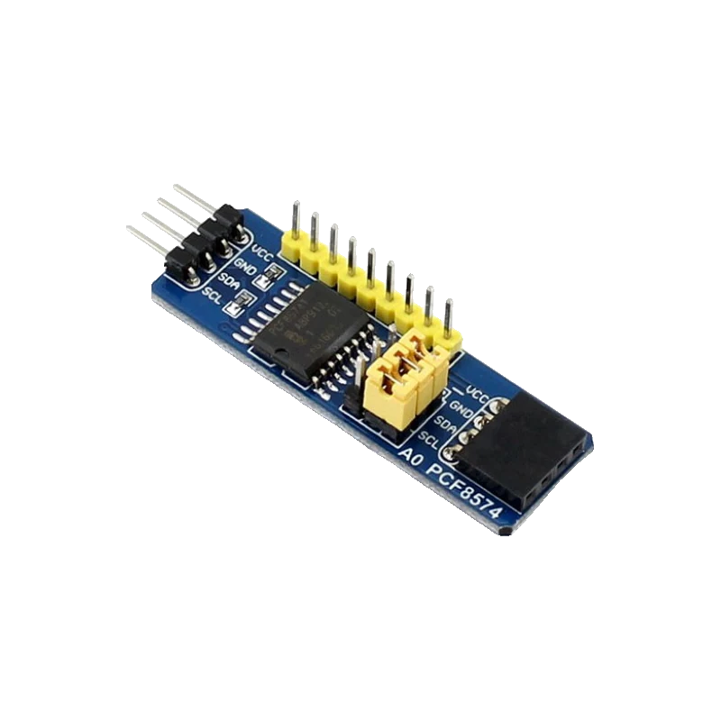
The PCF8574 adds eight I/O pins over I2C: it runs from 2.5 V to 6 V and answers at 0x20 to 0x27, set by its A0 to A2 pins (TI PCF8574 datasheet SCPS068K, pp. 1, 14), while the PCF8574A variant uses 0x38 to 0x3F (NXP PCF8574/74A datasheet Rev. 5, p. 6). Its pins sink up to 25 mA but source only a weak current, so wire LEDs from VCC into the pin and drive them low. The common blue expansion board puts 1 kOhm pull-ups on SDA and SCL to VCC (Waveshare PCF8574 schematic), so power it from 3.3 V on an ESP32 or Pico.
The PCF8574 is the simplest I2C port expander: one byte written sets all eight pins, one byte read returns them. Its I/O is quasi-bidirectional, which means there is no direction register. A pin written 0 pulls hard to ground (up to 25 mA recommended, TI datasheet p. 4); a pin written 1 is held high only by a weak current source, and anything outside can pull it low, which is how you read buttons.
That design shapes the wiring. LEDs and relay inputs go between VCC and the pin and switch on when you write 0. Buttons go from the pin to GND, and you write 1 to the pin before reading it. The chip has an open-drain INT output that falls when any input changes, so you do not need to poll.
The blue expansion board sold by Waveshare and copied widely brings P0 to P7 and INT to a header, has jumpers for A0 to A2, and passes I2C through to a second connector so several boards chain on one bus. Its schematic shows 1 kOhm pull-ups on SDA and SCL to VCC, which is why the board's supply must match your controller's logic level.
PCF8574 pinout
| Pin | Function | Type |
|---|---|---|
| VCC | VCC3.3 V or 5 V, equal to your board's logic level | power in |
| GND | GND | power in |
| SDA | I2C SDAPulled up to VCC through 1 kOhm | bidirectional |
| SCL | I2C SCLPulled up to VCC through 1 kOhm | input |
| P0 | GPIO | bidirectional |
| P1 | GPIO | bidirectional |
| P2 | GPIO | bidirectional |
| P3 | GPIO | bidirectional |
| P4 | GPIO | bidirectional |
| P5 | GPIO | bidirectional |
| P6 | GPIO | bidirectional |
| P7 | GPIO | bidirectional |
| INT | Interrupt (active low) | open collector |
| A0 | Address select | input |
| A1 | Address select | input |
| A2 | Address select | input |
How to wire the PCF8574
Pin by pin, for the board you have.
| PCF8574 | Arduino Uno | Note |
|---|---|---|
| VCC | 5V | |
| GND | GND | |
| SDA | A4 | |
| SCL | A5 | |
| A0 | GND jumper | A0, A1 and A2 all on the GND side: address 0x20. |
| P0 | LED cathode | LED anode to 5V through a 330 ohm resistor; the LED lights when P0 is written LOW. |
| P1 | Push button to GND | No resistor needed: the pin's own weak pull-up holds it high. |
| INT | D2 | Optional; use INPUT_PULLUP. |
| PCF8574 | ESP32 DevKit V1 | Note |
|---|---|---|
| VCC | 3V3 | |
| GND | GND | |
| SDA | GPIO21 (D21) | |
| SCL | GPIO22 (D22) | |
| A0 | GND jumper | A0, A1 and A2 on GND: address 0x20. |
| P0 | LED cathode | LED anode to 3V3 through a 150 ohm resistor; lights when P0 is LOW. |
| P1 | Push button to GND | |
| INT | GPIO27 (D27) | Optional; use INPUT_PULLUP. |
- Power the board from 3V3, never 5 V: its 1 kOhm pull-ups would put 5 V on GPIO21 and GPIO22.
- Anything wired to P0 to P7 must stay at 3.3 V too, since the pins only tolerate VCC + 0.5 V (TI datasheet, p. 4).
| PCF8574 | Raspberry Pi Pico | Note |
|---|---|---|
| VCC | 3V3(OUT) | |
| GND | GND | |
| SDA | GP4 | |
| SCL | GP5 | |
| A0 | GND jumper | A0, A1 and A2 on GND: address 0x20. |
| P0 | LED cathode | LED anode to 3V3(OUT) through a 150 ohm resistor; lights when P0 is LOW. |
| P1 | Push button to GND | |
| INT | GP6 | Optional; use INPUT_PULLUP. |
- Power the board from 3V3(OUT), never VBUS or VSYS: the 1 kOhm pull-ups follow VCC.
PCF8574 code
Every example here compiles for its board.
// PCF8574 on Arduino Uno: wiring and a free simulation at https://www.tinkered.ai/components/pcf8574
// PCF8574 board on an Arduino Uno: VCC 5V, SDA A4, SCL A5, address 0x20
// P0: LED from 5V through 330 ohm (on when LOW). P1: button to GND.
#include <Wire.h>
#include <PCF8574.h>

PCF8574 pcf(0x20);

void setup() {
  Serial.begin(115200);
  Wire.begin();
  if (!pcf.begin()) {          // writes 0xFF: every pin high (inputs ready, LED off)
    Serial.println("PCF8574 not found at 0x20. Check wiring and the A0-A2 jumpers.");
    while (true) delay(10);
  }
  Serial.println("PCF8574 ready");
}

void loop() {
  uint8_t pressed = (pcf.read(1) == LOW); // button pulls P1 low
  pcf.write(0, pressed ? LOW : HIGH);     // LED on while the button is held
  Serial.print("Button: ");
  Serial.println(pressed ? "pressed" : "released");
  delay(200);
}
// PCF8574 on ESP32 DevKit V1: wiring and a free simulation at https://www.tinkered.ai/components/pcf8574
// PCF8574 board on an ESP32 DevKit V1: VCC 3V3, SDA GPIO21, SCL GPIO22, address 0x20
// P0: LED from 3V3 through 150 ohm (on when LOW). P1: button to GND.
#include <Wire.h>
#include <PCF8574.h>

PCF8574 pcf(0x20);

void setup() {
  Serial.begin(115200);
  Wire.begin(21, 22);
  if (!pcf.begin()) {          // writes 0xFF: every pin high (inputs ready, LED off)
    Serial.println("PCF8574 not found at 0x20. Check wiring and the A0-A2 jumpers.");
    while (true) delay(10);
  }
  Serial.println("PCF8574 ready");
}

void loop() {
  bool pressed = (pcf.read(1) == LOW);
  pcf.write(0, pressed ? LOW : HIGH);
  Serial.printf("Button: %s\n", pressed ? "pressed" : "released");
  delay(200);
}
// PCF8574 on Raspberry Pi Pico: wiring and a free simulation at https://www.tinkered.ai/components/pcf8574
// PCF8574 board on a Raspberry Pi Pico (arduino-pico): VCC 3V3(OUT), SDA GP4, SCL GP5, address 0x20
// P0: LED from 3V3 through 150 ohm (on when LOW). P1: button to GND.
#include <Wire.h>
#include <PCF8574.h>

PCF8574 pcf(0x20, &Wire);

void setup() {
  Serial.begin(115200);
  Wire.setSDA(4);
  Wire.setSCL(5);
  Wire.begin();
  if (!pcf.begin()) {          // writes 0xFF: every pin high (inputs ready, LED off)
    Serial.println("PCF8574 not found at 0x20. Check wiring and the A0-A2 jumpers.");
    while (true) delay(10);
  }
  Serial.println("PCF8574 ready");
}

void loop() {
  bool pressed = (pcf.read(1) == LOW);
  pcf.write(0, pressed ? LOW : HIGH);
  Serial.print("Button: ");
  Serial.println(pressed ? "pressed" : "released");
  delay(200);
}
Before you wire it
- Power the board at your controller's logic voltage: its SDA and SCL pull-ups go to VCC (Waveshare schematic).
- Wire LEDs and active-low inputs between VCC and the pin, and turn them on by writing 0: the pin sinks up to 25 mA but sources only 30 to 310 µA (TI datasheet, pp. 4, 5).
- Write 1 to a pin before reading it as an input, so the weak pull-up holds it high until something pulls it low.
- Set A0 to A2 with the jumpers; each board on the bus needs its own address, 0x20 to 0x27 (TI datasheet, p. 14).
- Keep the bus at 100 kHz or slower (datasheet, p. 5).
- Never drive an LED from a high pin to GND: the weak source current gives at most a faint glow.
- Never exceed 100 mA through the chip's VCC or GND pin in total (datasheet, p. 4), even with each pin under 25 mA.
- Never power the board from 5 V on an ESP32 or Pico.
- Never leave A0, A1 or A2 floating; the datasheet asks for a direct connection to VCC or GND (p. 3).
- Quasi-bidirectional means each pin is an open-drain low with a weak current source high; a strong 1 mA pull-up is switched on only briefly after each write so the edge rises fast (TI datasheet, p. 5).
- INT is open drain and falls on any edge of a pin in input mode; reading or writing the port, or the pin returning to its old level, releases it (TI datasheet, p. 12).
- The 1 kOhm pull-ups on the expansion board are strong. Chaining several boards puts them in parallel; above two boards, remove some pull-ups so the controller can still pull the lines low.
- If a scanner finds the board at 0x38 to 0x3F, it carries the PCF8574A; the code is the same with that address (NXP datasheet, p. 6).
- On an Uno the 5 V version works directly; on 3.3 V boards, drive relay modules or 5 V loads from the PCF8574 only by sinking current through them to ground.
Specifications
- Supply voltage
- 2.5 V to 6 VTI PCF8574 datasheet SCPS068K, p. 4
- Absolute maximum supply
- 6.5 VTI PCF8574 datasheet SCPS068K, p. 4
- I2C address
- 0x20 to 0x27 (A2 A1 A0 = 000 to 111)TI PCF8574 datasheet SCPS068K, p. 14
- PCF8574A address
- 0x38 to 0x3FNXP PCF8574/PCF8574A datasheet Rev. 5 (27 May 2013), p. 6
- I2C clock
- 100 kHz maximumTI PCF8574 datasheet SCPS068K, p. 5
- Pin sink current
- 25 mA per pin recommended maximum; 100 mA total through VCC or GND (absolute)TI PCF8574 datasheet SCPS068K, p. 4
- Pin high drive
- Weak current source, 30 µA to 310 µA into a grounded pin; about 1 mA briefly after an acknowledgeTI PCF8574 datasheet SCPS068K, p. 5
- Standby current
- 2.5 µA typical, 10 µA maximumTI PCF8574 datasheet SCPS068K, p. 5
- Board pull-ups
- 1 kOhm on SDA and SCL to the board's VCCWaveshare PCF8574 IO Expansion Board schematic
From the PCF8574 Remote 8-Bit I/O Expander for I2C Bus, SCPS068K (revised September 2024), published by Texas Instruments / NXP.
Common mistakes
Expecting it to source current like a GPIO
A high PCF8574 pin supplies only about 30 to 310 µA (TI datasheet, p. 5). An LED wired from the pin to GND barely lights. Wire it from VCC through a resistor into the pin and write 0 to switch it on.
Confusing it with an LCD backpack
The I2C backpack on 1602 LCDs uses the same chip, so it shows up at 0x27 or 0x3F. This expansion board is a bare eight-pin port; a LiquidCrystal_I2C sketch won't drive it.
Wrong address for the A version
A board that won't answer at 0x20 to 0x27 may carry a PCF8574A, which lives at 0x38 to 0x3F (NXP datasheet, p. 6). Run an I2C scanner before suspecting the wiring.
Reading a pin you last wrote 0
A pin set low pulls itself to ground and always reads 0. Write 1 to every pin you want as an input; begin() in the robtillaart library starts with all pins high.
PCF8574 questions
What is the PCF8574's I2C address?
0x20 with A0, A1 and A2 all low, up to 0x27 with all three high (TI datasheet, p. 14). The PCF8574A version uses 0x38 to 0x3F (NXP datasheet, p. 6). Up to eight of each can share one bus.
PCF8574 or MCP23017?
The PCF8574 is simpler: eight pins, no registers, one byte in or out. The MCP23017 gives sixteen pins with real push-pull outputs, direction registers and internal pull-ups, and runs I2C up to 1.7 MHz. Pick the MCP23017 when outputs must source current or you need more pins.
Can the PCF8574 drive a relay module?
Yes, for the common active-low relay boards: their input is an LED from VCC to the IN pin, which the PCF8574 sinks when you write 0. On a 3.3 V board, power the PCF8574 from 3.3 V and check the relay board's own threshold.
Does the PCF8574 work at 3.3 V?
Yes, it runs from 2.5 V to 6 V (TI datasheet, p. 4). On an ESP32 or Pico, power the board from 3.3 V so its I2C pull-ups and its pins stay at 3.3 V.
Which library should I use?
Rob Tillaart's PCF8574 library (robtillaart/PCF8574) is small and works on AVR, ESP32 and RP2040. Call Wire.begin() first, then begin(), and use read(pin) and write(pin, value) or read8() and write8() for the whole port.
Build something with the PCF8574
- Build this
Eight-button panel
Read eight buttons over two wires with an interrupt on any press.
- Build this
Relay controller
Switch a four-channel relay board from an expander to free up GPIOs.
- Build this
LED bar graph
Show a sensor value on eight LEDs.
This page as plain Markdown, for ChatGPT, Claude or your own agent. /components/pcf8574.md