ADS1115 16-Bit ADC
A 16-bit, four-input I2C analog-to-digital converter with a programmable gain amplifier, from ±0.256 V to ±6.144 V full scale.
- Resolution16 bits, two's complement output
- Supply voltage2.0 V to 5.5 V
- Supply current150 µA typical (200 µA max) converting; 0.5 µA typical powered down
- Full-scale ranges (PGA)±6.144, ±4.096, ±2.048 (default), ±1.024, ±0.512, ±0.256 V
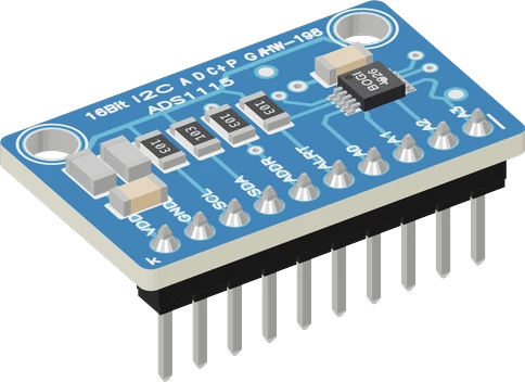
The ADS1115 is a 16-bit I2C analog-to-digital converter with four inputs, a programmable gain amplifier from ±0.256 V to ±6.144 V full scale, and 8 to 860 samples per second, running from 2.0 V to 5.5 V on 150 µA (TI ADS111x datasheet SBAS444E, pp. 1, 5, 6). Wire VDD to your board's logic voltage, GND to GND, SDA and SCL to the I2C pins, and leave ADDR on GND for address 0x48 (p. 20). Keep every input between GND - 0.3 V and VDD + 0.3 V whatever the gain (p. 4).
The ADS1115 is Texas Instruments' precision 16-bit delta-sigma ADC with an I2C interface, an internal voltage reference, an oscillator and a programmable gain amplifier (PGA) (TI datasheet SBAS444E, p. 1). The common blue HW-198 breakout puts it on a 1x10 header (VDD, GND, SCL, SDA, ADDR, ALRT, A0 to A3) with 10 kΩ pull-ups on SDA, SCL and ALRT. Makers reach for it when a microcontroller's own ADC is too coarse or too noisy: an Uno's ADC is 10-bit, and the ADS1115 resolves 7.8125 µV per code at its most sensitive range (p. 15).
The four inputs read single-ended against GND or as differential pairs. The PGA sets the full-scale range to ±6.144 V, ±4.096 V, ±2.048 V, ±1.024 V, ±0.512 V or ±0.256 V, with LSB sizes from 187.5 µV down to 7.8125 µV (p. 15). The chip resets to ±2.048 V, single-shot mode and 128 SPS (config register reset value 8583h, pp. 25, 26). The full-scale range is a scaling only: no input may go past VDD + 0.3 V, so on a 3.3 V supply the ±4.096 V range measures up to 3.3 V and the top codes are never reached (p. 15).
Data rate is programmable from 8 to 860 SPS (p. 5). In single-shot mode the chip converts once and powers down, drawing 0.5 µA typical between conversions (p. 6), which suits battery projects. The ALERT/RDY pin is an open-drain output that works as a window or traditional comparator, or gives an 8 µs conversion-ready pulse at the end of each conversion in continuous mode (pp. 16, 17). One ADDR pin selects four addresses, so up to four ADS1115s share one bus (p. 20).
ADS1115 16-Bit ADC pinout
| Pin | Function | Type |
|---|---|---|
| VDD | VDD: 2.0-5.5 V (through a ferrite bead)2–5 V | power in |
| GND | GND (through a ferrite bead) | power in |
| SCL | I2C SCL | bidirectional |
| SDA | I2C SDA | bidirectional |
| ADDR | Digital | input |
| ALRT | Digital | open collector |
| A0 | ADC AIN0 | input |
| A1 | ADC AIN1 | input |
| A2 | ADC AIN2 | input |
| A3 | ADC AIN3 | input |
How to wire the ADS1115 16-Bit ADC
Pin by pin, for the board you have.
| ADS1115 16-Bit ADC | Arduino Uno | Note |
|---|---|---|
| VDD | 5V | |
| GND | GND | |
| SDA | SDA | |
| SCL | SCL |
| ADS1115 16-Bit ADC | ESP32 DevKit V1 | Note |
|---|---|---|
| VDD | 3V3 | |
| GND | GND | |
| SDA | GPIO21 (D21) | |
| SCL | GPIO22 (D22) |
| ADS1115 16-Bit ADC | Raspberry Pi Pico | Note |
|---|---|---|
| VDD | 3V3 | |
| GND | GND | |
| SDA | GP4 | |
| SCL | GP5 |
ADS1115 16-Bit ADC code
Every example here compiles for its board.
// ADS1115 16-Bit ADC on Arduino Uno: wiring and a free simulation at https://www.tinkered.ai/components/ads1115-adc
#include <Arduino.h>
#include <Wire.h>
#include <Adafruit_ADS1X15.h>

Adafruit_ADS1115 ads;

void setup() {
  Serial.begin(115200);
  if (!ads.begin(0x48)) {
    Serial.println("ADS1115 not found: check VDD, SDA/SCL and the ADDR wiring");
    while (true) delay(10);
  }
  ads.setGain(GAIN_TWOTHIRDS);
}

void loop() {
  int16_t pot = ads.readADC_SingleEnded(0);
  int16_t tmp = ads.readADC_SingleEnded(1);
  float potV = ads.computeVolts(pot);
  float tempC = (ads.computeVolts(tmp) - 0.5f) * 100.0f;   // TMP36: 0.5 V at 0 °C, 10 mV/°C
  Serial.print("pot "); Serial.print(potV, 4); Serial.print(" V  ");
  Serial.print("temp "); Serial.print(tempC, 2); Serial.println(" C");
  delay(500);
}
// ADS1115 16-Bit ADC on ESP32 DevKit V1: wiring and a free simulation at https://www.tinkered.ai/components/ads1115-adc
#include <Arduino.h>
#include <Wire.h>
#include <Adafruit_ADS1X15.h>

Adafruit_ADS1115 ads;

void setup() {
  Serial.begin(115200);
  if (!ads.begin(0x48)) {
    Serial.println("ADS1115 not found: check VDD, SDA/SCL and the ADDR wiring");
    while (true) delay(10);
  }
  ads.setGain(GAIN_TWOTHIRDS);
}

void loop() {
  int16_t pot = ads.readADC_SingleEnded(0);
  int16_t tmp = ads.readADC_SingleEnded(1);
  float potV = ads.computeVolts(pot);
  float tempC = (ads.computeVolts(tmp) - 0.5f) * 100.0f;   // TMP36: 0.5 V at 0 °C, 10 mV/°C
  Serial.print("pot "); Serial.print(potV, 4); Serial.print(" V  ");
  Serial.print("temp "); Serial.print(tempC, 2); Serial.println(" C");
  delay(500);
}
// ADS1115 16-Bit ADC on Raspberry Pi Pico: wiring and a free simulation at https://www.tinkered.ai/components/ads1115-adc
#include <Arduino.h>
#include <Wire.h>
#include <Adafruit_ADS1X15.h>

Adafruit_ADS1115 ads;

void setup() {
  Serial.begin(115200);
  if (!ads.begin(0x48)) {
    Serial.println("ADS1115 not found: check VDD, SDA/SCL and the ADDR wiring");
    while (true) delay(10);
  }
  ads.setGain(GAIN_TWOTHIRDS);
}

void loop() {
  int16_t pot = ads.readADC_SingleEnded(0);
  int16_t tmp = ads.readADC_SingleEnded(1);
  float potV = ads.computeVolts(pot);
  float tempC = (ads.computeVolts(tmp) - 0.5f) * 100.0f;   // TMP36: 0.5 V at 0 °C, 10 mV/°C
  Serial.print("pot "); Serial.print(potV, 4); Serial.print(" V  ");
  Serial.print("temp "); Serial.print(tempC, 2); Serial.println(" C");
  delay(500);
}
Before you wire it
- VDD to the microcontroller board's logic supply (3V3 on an ESP32, a Pico, an STM32; 5V on an Uno), GND to its GND. Wire SDA/SCL to its I2C pins (Uno A4/A5, ESP32 GPIO21/22, Pico GP4/GP5, Nucleo D14/D15, NodeMCU D2/D1). No extra pull-ups: the module has 10 kΩ on both.
- Keep every input between 0 V and VDD.
- A sensor or potentiometer feeding an input runs from the module's VDD, not from a higher rail.
- Set the gain so the signal's largest value fits.
- In code: ads.begin(0x48) (the address from the ADDR wiring) and check it returned true. Call ads.setGain(...) before reading. ads.readADC_SingleEnded(n) returns the code; ads.computeVolts(code) gives volts at the current gain.
- Two modules: each its own address (ADDR wiring) and its own Adafruit_ADS1115 object, begin(0x49) and so on.
- Name your own constants without the library's names. Adafruit_ADS1X15.h #defines ADS1X15_ADDRESS, every ADS1X15_REG_* and RATE_ADS1115_*/RATE_ADS1015_*, and declares the enum GAIN_TWOTHIRDS...GAIN_SIXTEEN. A constant named the same breaks the build in the library's header. Use names of your own: ADC_ADDR, ADC_GAIN, BATTERY_DIVIDER.
- No input above VDD + 0.3 V or below GND - 0.3 V: a 5 V signal into a module on 3.3 V, a battery straight into an input.
- No VDD above the microcontroller board's logic voltage on a 3.3 V board: the pull-ups would put VDD on SDA/SCL.
- No ADDR wired to a GPIO: the chip reads ADDR continuously, so the address would move.
- No analogRead() on the module's inputs: they are the ADS1115's, read over I2C.
- Power VDD from your microcontroller board's logic voltage: 3.3 V on an ESP32, Pico or STM32, 5 V on an Uno. The chip accepts 2.0 V to 5.5 V (TI datasheet, p. 1), and the HW-198 module's 10 kΩ SDA and SCL pull-ups go to VDD, so VDD sets the bus's logic level.
- No input may go below GND - 0.3 V or above VDD + 0.3 V (p. 4). The ±6.144 V range does not let a module on 3.3 V read 5 V; scale higher voltages (a 12 V battery) down with a resistor divider of 100 kΩ or less.
- Pick the gain so the largest signal fits. On VDD = 3.3 V, ±4.096 V covers a 0 to 3.3 V signal; on 5 V, ±6.144 V covers 0 to 5 V (p. 15). Small signals such as a shunt or a bridge take ±0.512 V or ±0.256 V.
- ADDR selects the address: GND 0x48, VDD 0x49, SDA 0x4A, SCL 0x4B (p. 20). The module pulls ADDR down, so left open it answers at 0x48. TI asks to use GND, VDD and SCL first, since the SDA address needs SDA held low 100 ns after SCL falls (p. 20).
- ALRT (ALERT/RDY) is open drain with a pull-up on the module. Wire it to an interrupt pin to be told when a conversion finishes instead of polling (p. 17). The pin is not needed for basic reads.
- Tie unused inputs to GND, or never read them: an open input floats and reads random values.
- Differential input impedance is 4.9 MΩ at ±2.048 V.
Specifications
- Resolution
- 16 bits, two's complement outputTI ADS111x datasheet SBAS444E, pp. 1, 23
- Supply voltage
- 2.0 V to 5.5 VTI ADS111x datasheet SBAS444E, p. 1
- Supply current
- 150 µA typical (200 µA max) converting; 0.5 µA typical powered downTI ADS111x datasheet SBAS444E, p. 6
- Full-scale ranges (PGA)
- ±6.144, ±4.096, ±2.048 (default), ±1.024, ±0.512, ±0.256 VTI ADS111x datasheet SBAS444E, pp. 15, 26
- LSB size
- 187.5 µV at ±6.144 V down to 7.8125 µV at ±0.256 VTI ADS111x datasheet SBAS444E, p. 15
- Data rate
- 8, 16, 32, 64, 128 (default), 250, 475, 860 SPSTI ADS111x datasheet SBAS444E, pp. 5, 26
- Analog input limit
- GND - 0.3 V to VDD + 0.3 V, whatever the gainTI ADS111x datasheet SBAS444E, p. 4
- Accuracy
- Gain error 0.01 % typical (0.15 % max), INL 1 LSB max at 8 SPSTI ADS111x datasheet SBAS444E, p. 5
- I2C addresses
- 0x48 (ADDR to GND), 0x49 (VDD), 0x4A (SDA), 0x4B (SCL)TI ADS111x datasheet SBAS444E, p. 20
- Operating temperature
- -40 °C to +125 °CTI ADS111x datasheet SBAS444E, p. 1
- Maximum supply voltage
- 5.5 V
- Interface
- I2C
- I2C address
- 0x48
- On-board I2C pull-ups
- Yes (10 kΩ)
- Dimensions
- 28 × 17 × 11.5 mm
- Weight
- 2 g
From the Texas Instruments ADS1115 (generic HW-198 module)'s datasheet, published by Texas Instruments ADS1115 (generic HW-198 module).
Common mistakes
Expecting ±6.144 V to read 5 V on a 3.3 V supply
The full-scale range is only the ADC's scaling. The inputs are still limited to VDD + 0.3 V (TI datasheet, p. 4), and above that the chip's protection diodes clamp the signal. Power the ADS1115 from 5 V for 0 to 5 V signals, or divide the signal down.
Reading stuck at 32767
The input is above the selected full-scale range, so the code saturates at 7FFFh (p. 23). Choose a lower gain (a wider range) or divide the signal.
Wrong address in begin()
The address follows what ADDR is wired to: 0x48 on GND or open on the module, 0x49 on VDD, 0x4A on SDA, 0x4B on SCL (p. 20). An I2C scanner shows which one the board answers at.
Divider resistors in the megohms
The inputs have a finite impedance, 4.9 MΩ differential at ±2.048 V and 710 kΩ at ±0.512 V and ±0.256 V (p. 5). A high-value divider sags under that load and reads low. Keep divider resistors at 100 kΩ or below, or buffer the signal.
Slow loop from single-shot reads
Each single-shot read waits for one conversion: about 8 ms at the default 128 SPS. Raise the data rate up to 860 SPS (p. 5), or use continuous mode with the ALRT conversion-ready pulse (p. 17).
ADS1115 16-Bit ADC questions
Can I use the ADS1115 with 3.3 V and 5 V boards?
Yes. The chip runs from 2.0 V to 5.5 V (TI datasheet, p. 1). Power the module from the board's own logic voltage so its 10 kΩ pull-ups hold SDA and SCL at that level. The analog inputs then accept 0 V to VDD (VDD + 0.3 V absolute maximum, p. 4).
What is the ADS1115 I2C address?
0x48 with ADDR on GND, which is what the HW-198 module gives when ADDR is left open. Wiring ADDR to VDD, SDA or SCL gives 0x49, 0x4A or 0x4B, so four ADS1115s can share one bus (TI datasheet, p. 20).
Which gain should I use on the ADS1115?
The smallest range that still holds your largest signal. ±4.096 V (GAIN_ONE) suits 0 to 3.3 V signals, ±6.144 V (GAIN_TWOTHIRDS) suits 0 to 5 V on a 5 V supply, and ±0.256 V gives 7.8125 µV steps for small signals (TI datasheet, p. 15). A single-ended reading uses the positive half, codes 0 to 32767.
Why does my ADS1115 read wrong or not at all?
If begin() fails, check VDD, GND, the SDA and SCL pins, and that the address in your code matches the ADDR wiring (TI datasheet, p. 20). If readings stop at 32767, the input is past the selected range (p. 23); if they wander, the input is floating. A reading that never rises past about VDD means the input is above VDD + 0.3 V and is being clamped (p. 4).
ADS1115 vs ADS1015: what is the difference?
Both share the same pinout and I2C addresses. The ADS1115 is 16-bit with data rates of 8 to 860 SPS (TI ADS111x datasheet, pp. 1, 5); the ADS1015 is TI's 12-bit sibling, faster but coarser. Pick the ADS1115 for precise slow signals such as batteries, load cells through an amplifier, or thermocouple amplifiers.
How fast can the ADS1115 sample?
Up to 860 samples per second, set in steps of 8, 16, 32, 64, 128, 250, 475 and 860 SPS (TI datasheet, p. 5). Lower rates average more and give lower noise. At 860 SPS a single conversion takes about 1.2 ms (p. 18).
Build something with the ADS1115 16-Bit ADC
- Build this
Battery voltage monitor
Read a 12 V battery through a resistor divider with far finer steps than the board's own ADC.
- Build this
Precision potentiometer or joystick input
Four channels of 16-bit position readings for a control panel or camera slider.
- Build this
Solar panel logger
Log panel voltage and current through a shunt, reading the shunt on a high-gain range.
- Build this
Analog sensor hub for an ESP32
Replace the ESP32's non-linear ADC with four clean inputs for soil, light and gas sensors.
This page as plain Markdown, for ChatGPT, Claude or your own agent. /components/ads1115-adc.md