74HC595 Shift Register with an ESP32 DevKit V1
The 74HC595 is an 8-bit serial-in, parallel-out shift register that turns three microcontroller pins into eight latched outputs.
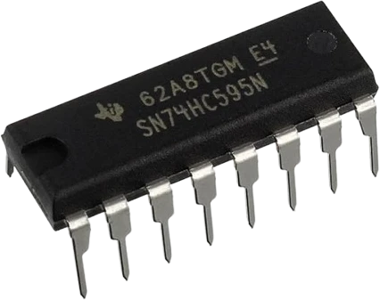
On the ESP32 DevKit V1 the 74HC595 takes VCC and SRCLR from the 3V3 pin, so the chip and the ESP32 share one logic rail and every output swings between GND and 3.3 V. SER, SRCLK and RCLK sit on GPIO13, GPIO14 and GPIO27, three pins the ESP32 does not read at reset, and shiftOut() clocks each byte out in software before RCLK latches it.
Wiring the 74HC595 Shift Register to the ESP32 DevKit V1
Pin by pin.
| 74HC595 Shift Register | ESP32 DevKit V1 |
|---|---|
| VCC | 3V3 |
| GND | GND |
| SER | GPIO13 (D13) |
| SRCLK | GPIO14 (D14) |
| RCLK | GPIO27 (D27) |
| SRCLR | 3V3 |
| OE | GND |
What to know on the ESP32 DevKit V1
- Keep VCC on 3V3 rather than VIN. TI sets the high input threshold at 0.7 x VCC (3.15 V with a 4.5 V supply), while an ESP32 output is only guaranteed to reach 0.8 x VDD, about 2.64 V, so a chip on 5 V could miss the ESP32's highs. On 3.3 V the threshold scales down to roughly 2.3 V, which the ESP32 clears.TI SN74HC595 datasheet SCLS041J, p. 4; Espressif ESP32 Series Datasheet v5.3, p. 52
- TI states the 6 mA output drive for a 4.5 V supply and only 20 µA at 2 V, with nothing in between, so on 3V3 size each LED resistor for a few milliamps. The 70 mA absolute limit through the VCC or GND pin covers all eight outputs together.TI SN74HC595 datasheet SCLS041J, pp. 4, 5
- GPIO13 and GPIO14 are also the ESP32's JTAG pins MTCK and MTMS, which only matters when a JTAG probe is attached. If you move the three lines, stay off GPIO0, GPIO2, GPIO5, GPIO12 and GPIO15: the chip latches their levels at reset to pick its boot mode and flash voltage.Espressif ESP32 Series Datasheet v5.3, pp. 14, 22
- To refresh a long chain faster, move SER to GPIO23 (VSPI data out) and SRCLK to GPIO18 (VSPI clock), send each byte with SPI.transfer() and pulse RCLK on GPIO27 afterwards. An SPI clock of 4 MHz or less stays under the 5 MHz TI guarantees even with the chip at 2 V.Espressif ESP32 Series Datasheet v5.3, p. 15; TI SN74HC595 datasheet SCLS041J, p. 6
74HC595 Shift Register code for the ESP32 DevKit V1
Compiled for esp32:esp32:esp32 on 2026-10-29.
// 74HC595 Shift Register on ESP32 DevKit V1: wiring and a free simulation at https://www.tinkered.ai/components/74hc595-shift-register/esp32
const int DATA_PIN  = 13;   // SER   (DS)
const int CLOCK_PIN = 14;   // SRCLK (SH_CP)
const int LATCH_PIN = 27;   // RCLK  (ST_CP)

void setup() {
  pinMode(DATA_PIN, OUTPUT);
  pinMode(CLOCK_PIN, OUTPUT);
  pinMode(LATCH_PIN, OUTPUT);
}

// MSBFIRST: bit 7 -> QH, bit 0 -> QA.
void writeByte(byte value) {
  digitalWrite(LATCH_PIN, LOW);
  shiftOut(DATA_PIN, CLOCK_PIN, MSBFIRST, value);
  digitalWrite(LATCH_PIN, HIGH);   // RCLK rising latches to QA..QH
}

void loop() {
  for (int i = 0; i < 8; i++) {    // walking 1: QA -> QH
    writeByte(1 << i);
    delay(150);
  }
}
74HC595 Shift Register on the ESP32 DevKit V1: questions
Can I power the 74HC595 from the ESP32's VIN pin?
Not with the ESP32 driving its inputs. On about 5 V the chip wants 3.15 V or more for a high at a 4.5 V supply (TI, p. 4), and the ESP32 guarantees only 0.8 x VDD, about 2.64 V (Espressif datasheet, p. 52). The page wires VCC and SRCLR to 3V3 so both sides use the same rail.
Can the 74HC595 outputs switch a 5 V load from an ESP32?
Not directly: QA to QH swing only to the chip's own supply, 3.3 V here. Put a transistor on each output that has to switch a 5 V load, and keep the 74HC595 itself on 3V3.
How do I chain two 74HC595s on the ESP32?
Wire the first chip's QH' (pin 9) to the second chip's SER and share SRCLK and RCLK on GPIO14 and GPIO27. Call shiftOut() once per chip, farthest chip first, then raise RCLK once to update all sixteen outputs together.
Keep going
This guide as plain Markdown. /components/74hc595-shift-register/esp32.md